您好,欢迎进入深圳市颖特新科技有限公司官方网站!
您好,欢迎进入深圳市颖特新科技有限公司官方网站!
今天来说说新唐库函数的写法讲解,一般来说,我们给寄存器定义地址或分配地址,无外乎就是宏定义或者结构体,而新塘呢,同样也是如此,作为C高级语言,一般上升到M0,M4就会有大量的寄存器和配置参数,但是相对来说,性能也会提高。
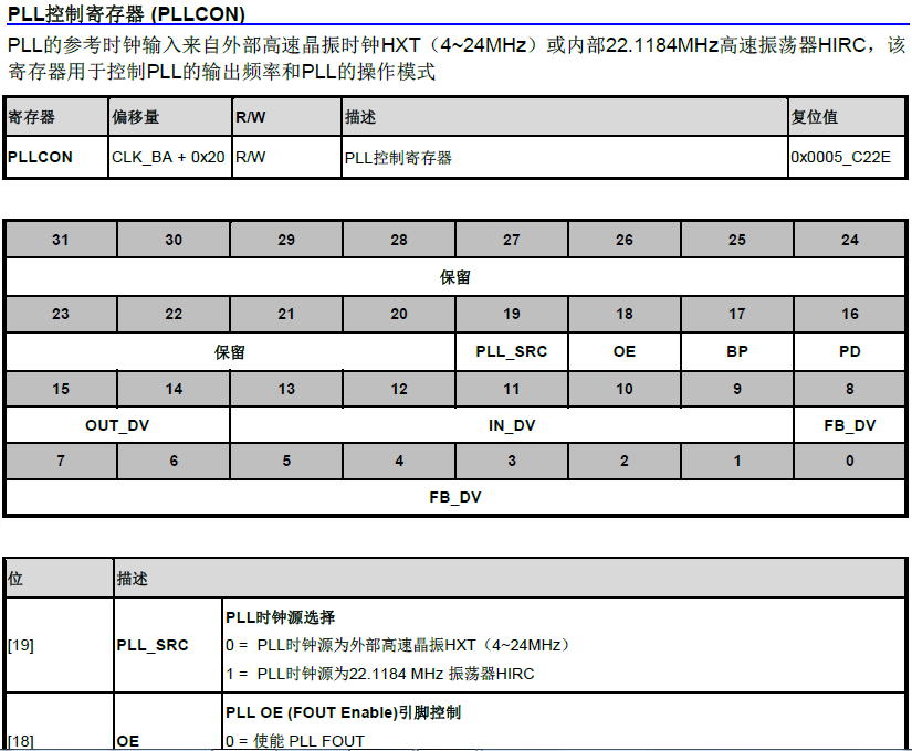
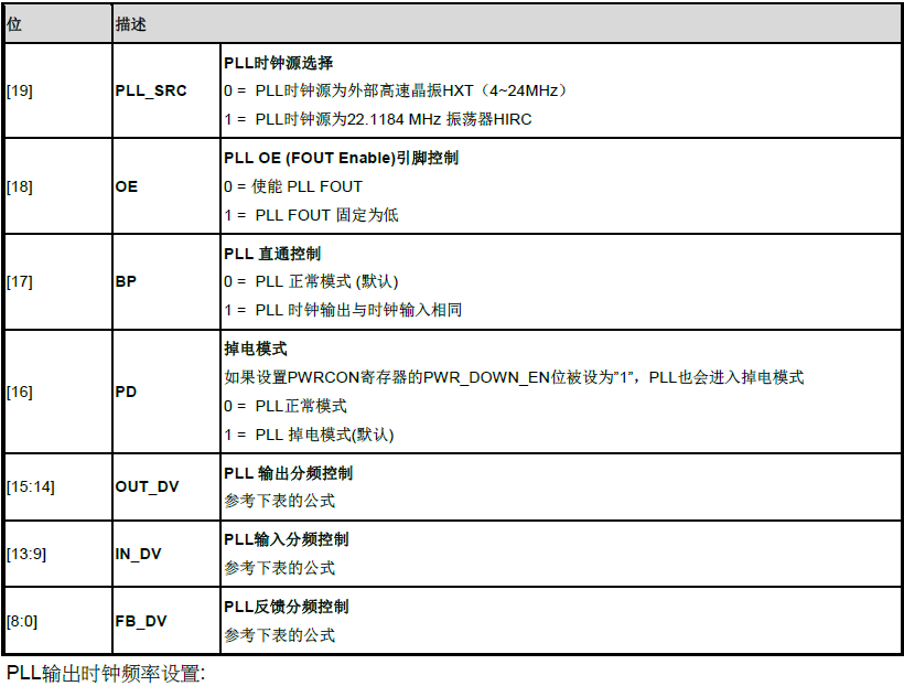
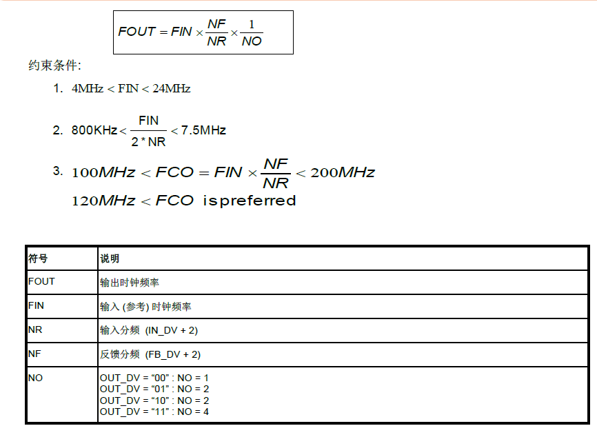
typedef struct { /** * PWRCON * =================================================================================================== * Offset: 0x00 System Power Down Control Register * --------------------------------------------------------------------------------------------------- * |Bits |Field |Descriptions * | :----: | :----: | :---- | * |[0] |XTL12M_EN |External Crystal Oscillator Control * | | |The bit default value is set by flash controller user configuration register config0 [26:24]. * | | |When the default clock source is from external crystal. The bit is auto set to "1" * | | |1 = Crystal oscillation enable * | | |0 = Crystal oscillation disable * |[2] |OSC22M_EN |Internal 22.1184 MHz Oscillator Control * | | |1 = 22.1184 MHz Oscillation enable * | | |0 = 22.1184 MHz Oscillation disable * |[3] |OSC10K_EN |Internal 10KHz Oscillator Control * | | |1 = 10KHz Oscillation enable * | | |0 = 10KHz Oscillation disable * |[4] |PD_WU_DLY |Enable the wake up delay counter. * | | |When the chip wakes up from power down mode, the clock control will delay certain clock * | | |cycles to wait system clock stable. * | | |The delayed clock cycle is 4096 clock cycles when chip work at external crystal (4 ~ * | | |24MHz), and 256 clock cycles when chip work at 22.1184 MHz oscillator. * | | |1 = Enable the clock cycle delay * | | |0 = Disable the clock cycle delay * |[5] |PD_WU_INT_EN|Power down mode wake Up Interrupt Enable * | | |0 = Disable * | | |1 = Enable. The interrupt will occur when Power down mode (Deep Sleep Mode) wakeup. * |[6] |PD_WU_STS |Chip power down wake up status flag * | | |Set by "power down wake up", it indicates that resume from power down mode * | | |The flag is set if the GPIO(P0~P4), UART wakeup * | | |Write 1 to clear the bit * | | |Note: This bit is working only if PD_WU_INT_EN (PWRCON[5]) set to 1. * |[7] |PWR_DOWN_EN |System power down enable bit * | | |When set this bit "1", the chip power down mode is enabled and the chip power down active * | | |is depend on the PD_WAIT_CPU bit * | | |(a) if the PD_WAIT_CPU is "0" then the chip power down after the PWR_DOWN_EN bit set. * | | |(b) if the PD_WAIT_CPU is "1" then the chip keep active till the CPU sleep mode also active * | | |and then the chip power down * | | |When chip wake up from power down, this bit is auto cleared, user need to set this bit again * | | |for next power down. * | | |When in power down mode, external crystal (4~ 24MHz) and the 22.1184 MHz OSC will be * | | |disabled in this mode, but the 10 kHz OSC is not controlled by power down mode. * | | |When in power down mode, the PLL and system clock are disabled, and ignored the clock * | | |source selection. The clocks of peripheral are not controlled by power down mode, if the * | | |peripheral clock source is from 10 kHz oscillator. * | | |1 = Chip enter the power down mode instant or wait CPU sleep command WFI * | | |0 = Chip operate in normal mode or CPU in idle mode (sleep mode) because of WFI * | | |command * |[8] |PD_WAIT_CPU |This bit control the power down entry condition * | | |1 = Chip entry power down mode when the both PWR_DOWN and CPU run WFI instruction. * | | |0 = Chip entry power down mode when the PWR_DOWN bit is set to 1 */ __IO uint32_t PWRCON; /** * AHBCLK * =================================================================================================== * Offset: 0x04 AHB Devices Clock Enable Control Register * --------------------------------------------------------------------------------------------------- * |Bits |Field |Descriptions * | :----: | :----: | :---- | * |[2] |ISP_EN |Flash ISP Controller Clock Enable Control. * | | |1 = To enable the Flash ISP controller clock. * | | |0 = To disable the Flash ISP controller clock. * |[3] |EBI_EN |EBI Controller Clock Enable Control. * | | |1 = To enable the EBI Controller clock. * | | |0 = To disable the EBI Controller clock. * |[4] |HDIV_EN |Divider Controller Clock Enable Control. * | | |1 = To enable the Divider Controller clock. * | | |0 = To disable the Divider Controller clock. */ __IO uint32_t AHBCLK; /** * APBCLK * =================================================================================================== * Offset: 0x08 APB Devices Clock Enable Control Register * --------------------------------------------------------------------------------------------------- * |Bits |Field |Descriptions * | :----: | :----: | :---- | * |[0] |WDT_EN |Watch Dog Timer Clock Enable. * | | |This bit is the protected bit, program this need a open lock sequence, write "59h","16h","88h" to * | | |address 0x5000_0100 to un-lock this bit. Reference the register REGWRPROT at address * | | |GCR_BA + 0x100 * | | |0 = Disable Watchdog Timer Clock * | | |1 = Enable Watchdog Timer Clock * |[2] |TMR0_EN |Timer0 Clock Enable Control * | | |0 = Disable Timer0 Clock * | | |1 = Enable Timer0 Clock * |[3] |TMR1_EN |Timer1 Clock Enable Control * | | |0 = Disable Timer1 Clock * | | |1 = Enable Timer1 Clock * |[4] |TMR2_EN |Timer2 Clock Enable Control * | | |0 = Disable Timer2 Clock * | | |1 = Enable Timer2 Clock * |[5] |TMR3_EN |Timer3 Clock Enable Control * | | |0 = Disable Timer3 Clock * | | |1 = Enable Timer3 Clock * |[6] |FDIV_EN |Clock Divider Clock Enable Control * | | |0 = Disable FDIV Clock * | | |1 = Enable FDIV Clock * |[8] |I2C_EN |I2C Clock Enable Control. * | | |0 = Disable I2C Clock * | | |1 = Enable I2C Clock * |[12] |SPI0_EN |SPI0 Clock Enable Control. * | | |0 = Disable SPI0 Clock * | | |1 = Enable SPI0 Clock * |[13] |SPI1_EN |SPI1 Clock Enable Control. * | | |0 = Disable SPI1 Clock * | | |1 = Enable SPI1 Clock * |[16] |UART0_EN |UART0 Clock Enable Control. * | | |1 = Enable UART0 clock * | | |0 = Disable UART0 clock * |[17] |UART1_EN |UART1 Clock Enable Control. * | | |1 = Enable UART1 clock * | | |0 = Disable UART1 clock * |[20] |PWM01_EN |PWM_01 Clock Enable Control. * | | |1 = Enable PWM01 clock * | | |0 = Disable PWM01 clock * |[21] |PWM23_EN |PWM_23 Clock Enable Control. * | | |1 = Enable PWM23 clock * | | |0 = Disable PWM23 clock * |[22] |PWM45_EN |PWM_45 Clock Enable Control. * | | |1 = Enable PWM45 clock * | | |0 = Disable PWM45 clock * |[23] |PWM67_EN |PWM_67 Clock Enable Control. * | | |1 = Enable PWM67 clock * | | |0 = Disable PWM67 clock * |[28] |ADC_EN |Analog-Digital-Converter (ADC) Clock Enable Control. * | | |1 = Enable ADC clock * | | |0 = Disable ADC clock */ __IO uint32_t APBCLK; /** * CLKSTATUS * =================================================================================================== * Offset: 0x0C Clock Status Monitor Register * --------------------------------------------------------------------------------------------------- * |Bits |Field |Descriptions * | :----: | :----: | :---- | * |[0] |XTL12M_STB |XTL12M clock source stable flag * | | |1 = External Crystal clock is stable * | | |0 = External Crystal clock is not stable or not enable * |[2] |PLL_STB |PLL clock source stable flag * | | |1 = PLL clock is stable * | | |0 = PLL clock is not stable or not enable * |[3] |OSC10K_STB |OSC10K clock source stable flag * | | |1 = OSC10K clock is stable * | | |0 = OSC10K clock is not stable or not enable * |[4] |OSC22M_STB |OSC22M clock source stable flag * | | |1 = OSC22M clock is stable * | | |0 = OSC22M clock is not stable or not enable * |[7] |CLK_SW_FAIL|Clock switch fail flag * | | |1 = Clock switch fail * | | |0 = Clock switch success * | | |This bit will be set when target switch clock source is not stable. Write 1 to clear this bit to zero. */ __IO uint32_t CLKSTATUS; /** * CLKSEL0 * =================================================================================================== * Offset: 0x10 Clock Source Select Control Register 0 * --------------------------------------------------------------------------------------------------- * |Bits |Field |Descriptions * | :----: | :----: | :---- | * |[2:0] |HCLK_S |HCLK clock source select. * | | |Note: * | | |1. Before clock switch the related clock sources (pre-select and new-select) must be turn on * | | |2. The 3-bit default value is reloaded with the value of Config0.CFOSC[26:24] in user * | | |configuration register in Flash controller by any reset. Therefore the default value is either * | | |000b or 111b. * | | |3. These bits are protected bit, program this need an open lock sequence, write * | | |"59h","16h","88h" to address 0x5000_0100 to un-lock this bit. Reference the register * | | |REGWRPROT at address GCR_BA + 0x100 * | | |000 = clock source from external crystal clock (4 ~ 24MHz) * | | |010 = clock source from PLL clock * | | |011 = clock source from internal 10KHz oscillator clock * | | |111 = clock source from internal 22.1184 MHz oscillator clock * | | |others = Reserved * |[5:3] |STCLK_S |MCU Cortex_M0 SysTick clock source select. * | | |These bits are protected bit, program this need an open lock sequence, write "59h","16h","88h" to * | | |address 0x5000_0100 to un-lock this bit. Reference the register REGWRPROT at address GCR_BA * | | |+ 0x100 * | | |000 = Clock source from external crystal clock (4 ~ 24MHz) * | | |010 = Clock source from external crystal clock (4 ~ 24MHz)/2 * | | |011 = clock source from HCLK/2 * | | |1xx = clock source from internal 22.1184 MHz oscillator clock/2 */ __IO uint32_t CLKSEL0; /** * CLKSEL1 * =================================================================================================== * Offset: 0x14 Clock Source Select Control Register 1 * --------------------------------------------------------------------------------------------------- * |Bits |Field |Descriptions * | :----: | :----: | :---- | * |[1:0] |WDT_S |Watchdog Timer clock source select. * | | |These bits are protected bit, program this need a open lock sequence, write "59h","16h","88h" to * | | |address 0x5000_0100 to un-lock this bit. Reference the register REGWRPROT at address * | | |GCR_BA + 0x100 * | | |00 = clock source from external crystal clock (4 ~ 24MHz). * | | |10 = clock source from HCLK/2048 clock * | | |11 = clock source from internal 10KHz oscillator clock * |[3:2] |ADC_S |ADC clock source select. * | | |00 = clock source from external crystal clock (4 ~ 24MHz). * | | |01 = clock source from PLL clock * | | |1x = clock source from internal 22.1184 MHz oscillator clock * |[10:8] |TMR0_S |TIMER0 clock source select. * | | |000 = clock source from external crystal clock (4 ~ 24MHz) * | | |010 = clock source from HCLK * | | |011 = clock source from external trigger * | | |1xx = clock source from internal 22.1184 MHz oscillator clock * |[14:12] |TMR1_S |TIMER1 clock source select. * | | |000 = clock source from external crystal clock (4 ~ 24MHz) * | | |010 = clock source from HCLK * | | |011 = clock source from external trigger * | | |1xx = clock source from internal 22.1184 MHz oscillator clock * |[18:16] |TMR2_S |TIMER2 clock source select. * | | |000 = clock source from external crystal clock (4 ~ 24MHz) * | | |010 = clock source from HCLK * | | |011 = clock source from external trigger * | | |1xx = clock source from internal 22.1184 MHz oscillator clock * |[22:20] |TMR3_S |TIMER3 clock source select. * | | |000 = clock source from external crystal clock (4 ~ 24MHz) * | | |010 = clock source from HCLK * | | |011 = clock source from external trigger * | | |1xx = clock source from internal 22.1184 MHz oscillator clock * |[25:24] |UART_S |UART clock source select. * | | |00 = clock source from external crystal clock (4 ~ 24MHz) * | | |01 = clock source from PLL clock * | | |1x = clock source from internal 22.1184 MHz oscillator clock * |[29:28] |PWM01_S |PWM0 and PWM1 clock source select. * | | |PWM0 and PWM1 uses the same Engine clock source, both of them with the same pre-scalar * | | |00 = clock source from external crystal clock (4 ~ 24MHz) * | | |10 = clock source from HCLK * | | |11 = clock source from internal 22.1184 MHz oscillator clock * |[31:30] |PWM23_S |PWM2 and PWM3 clock source select. * | | |PWM2 and PWM3 uses the same Engine clock source, both of them with the same pre-scalar * | | |00 = clock source from external crystal clock (4 ~ 24MHz) * | | |10 = clock source from HCLK * | | |11 = clock source from internal 22.1184 MHz oscillator clock */ __IO uint32_t CLKSEL1; /** * CLKDIV * =================================================================================================== * Offset: 0x18 Clock Divider Number Register * --------------------------------------------------------------------------------------------------- * |Bits |Field |Descriptions * | :----: | :----: | :---- | * |[3:0] |HCLK_N |HCLK clock divide number from HCLK clock source * | | |The HCLK clock frequency = (HCLK clock source frequency) / (HCLK_N + 1) * |[11:8] |UART_N |UART clock divide number from UART clock source * | | |The UART clock frequency = (UART clock source frequency ) / (UART_N + 1) * |[23:16] |ADC_N |ADC clock divide number from ADC clock source * | | |The ADC clock frequency = (ADC clock source frequency ) / (ADC_N + 1) */ __IO uint32_t CLKDIV; /** * CLKSEL2 * =================================================================================================== * Offset: 0x1C Clock Source Select Control Register 2 * --------------------------------------------------------------------------------------------------- * |Bits |Field |Descriptions * | :----: | :----: | :---- | * |[3:2] |FRQDIV_S |Clock Divider Clock Source Select * | | |00 = clock source from external crystal clock (4 ~ 24MHz) * | | |10 = clock source from HCLK * | | |11 = clock source from internal 22.1184 MHz oscillator clock * |[5:4] |PWM45_S |PWM4 and PWM5 clock source select. - PWM4 and PWM5 used the same Engine clock source, * | | |both of them with the same pre-scalar * | | |00 = clock source from external crystal clock (4 ~ 24MHz) * | | |10 = clock source from HCLK * | | |11 = clock source from internal 22.1184 MHz oscillator clock * |[7:6] |PWM67_S |PWM6 and PWM7 clock source select. - PWM6 and PWM7 used the same Engine clock source, * | | |both of them with the same pre-scalar * | | |00 = clock source from external crystal clock (4 ~ 24MHz) * | | |10 = clock source from HCLK * | | |11 = clock source from internal 22.1184 MHz oscillator clock */ __IO uint32_t CLKSEL2; /** * PLLCON * =================================================================================================== * Offset: 0x20 PLL Control Register * --------------------------------------------------------------------------------------------------- * |Bits |Field |Descriptions * | :----: | :----: | :---- | * |[8:0] |FB_DV |PLL Feedback Divider Control Pins (PLL_F[8:0]) * |[13:9] |IN_DV |PLL Input Divider Control Pins (PLL_R[4:0]) * |[15:14] |OUT_DV |PLL Output Divider Control Pins (PLL_OD[1:0]) * |[16] |PD |Power Down Mode. * | | |If set the IDLE bit "1" in PWRCON register, the PLL will enter power down mode too * | | |0 = PLL is in normal mode (default) * | | |1 = PLL is in power-down mode * |[17] |BP |PLL Bypass Control * | | |0 = PLL is in normal mode (default) * | | |1 = PLL clock output is same as clock input (XTALin) * |[18] |OE |PLL OE (FOUT enable) pin Control * | | |0 = PLL FOUT enable * | | |1 = PLL FOUT is fixed low * |[19] |PLL_SRC |PLL Source Clock Select * | | |1 = PLL source clock from 22.1184 MHz oscillator * | | |0 = PLL source clock from external crystal clock (4 ~ 24 MHz) */ __IO uint32_t PLLCON; /** * FRQDIV * =================================================================================================== * Offset: 0x24 Frequency Divider Control Register * --------------------------------------------------------------------------------------------------- * |Bits |Field |Descriptions * | :----: | :----: | :---- | * |[3:0] |FSEL |Divider Output Frequency Selection Bits * | | |The formula of output frequency is * | | |Fout = Fin/2(N+1), * | | |where Fin is the input clock frequency, Fout is the frequency of divider output clock, N is the 4-bit * | | |value of FSEL[3:0]. * |[4] |DIVIDER_EN|Frequency Divider Enable Bit * | | |0 = Disable Frequency Divider * | | |1 = Enable Frequency Divider */ __IO uint32_t FRQDIV; } CLK_T; /** @addtogroup CLK_CONST CLK Bit Field Definition Constant Definitions for CLK Controller @{ */ /* CLK PWRCON Bit Field Definitions */ #define CLK_PWRCON_PD_WAIT_CPU_Pos 8 /*!< CLK PWRCON: PD_WAIT_CPU Position */ #define CLK_PWRCON_PD_WAIT_CPU_Msk (1ul << CLK_PWRCON_PD_WAIT_CPU_Pos) /*!< CLK PWRCON: PD_WAIT_CPU Mask */ #define CLK_PWRCON_PWR_DOWN_EN_Pos 7 /*!< CLK PWRCON: PWR_DOWN_EN Position */ #define CLK_PWRCON_PWR_DOWN_EN_Msk (1ul << CLK_PWRCON_PWR_DOWN_EN_Pos) /*!< CLK PWRCON: PWR_DOWN_EN Mask */ #define CLK_PWRCON_PD_WU_STS_Pos 6 /*!< CLK PWRCON: PD_WU_STS Position */ #define CLK_PWRCON_PD_WU_STS_Msk (1ul << CLK_PWRCON_PD_WU_STS_Pos) /*!< CLK PWRCON: PD_WU_STS Mask */ #define CLK_PWRCON_PD_WU_INT_EN_Pos 5 /*!< CLK PWRCON: PD_WU_INT_EN Position */ #define CLK_PWRCON_PD_WU_INT_EN_Msk (1ul << CLK_PWRCON_PD_WU_INT_EN_Pos) /*!< CLK PWRCON: PD_WU_INT_EN Mask */ #define CLK_PWRCON_PD_WU_DLY_Pos 4 /*!< CLK PWRCON: PD_WU_DLY Position */ #define CLK_PWRCON_PD_WU_DLY_Msk (1ul << CLK_PWRCON_PD_WU_DLY_Pos) /*!< CLK PWRCON: PD_WU_DLY Mask */ #define CLK_PWRCON_OSC10K_EN_Pos 3 /*!< CLK PWRCON: OSC10K_EN Position */ #define CLK_PWRCON_OSC10K_EN_Msk (1ul << CLK_PWRCON_OSC10K_EN_Pos) /*!< CLK PWRCON: OSC10K_EN Mask */ #define CLK_PWRCON_IRC10K_EN_Pos 3 /*!< CLK PWRCON: OSC10K_EN Position */ #define CLK_PWRCON_IRC10K_EN_Msk (1ul << CLK_PWRCON_OSC10K_EN_Pos) /*!< CLK PWRCON: OSC10K_EN Mask */ #define CLK_PWRCON_OSC22M_EN_Pos 2 /*!< CLK PWRCON: OSC22M_EN Position */ #define CLK_PWRCON_OSC22M_EN_Msk (1ul << CLK_PWRCON_OSC22M_EN_Pos) /*!< CLK PWRCON: OSC22M_EN Mask */ #define CLK_PWRCON_IRC22M_EN_Pos 2 /*!< CLK PWRCON: OSC22M_EN Position */ #define CLK_PWRCON_IRC22M_EN_Msk (1ul << CLK_PWRCON_OSC22M_EN_Pos) /*!< CLK PWRCON: OSC22M_EN Mask */ #define CLK_PWRCON_XTL12M_EN_Pos 0 /*!< CLK PWRCON: XTL12M_EN Position */ #define CLK_PWRCON_XTL12M_EN_Msk (1ul << CLK_PWRCON_XTL12M_EN_Pos) /*!< CLK PWRCON: XTL12M_EN Mask */ /* CLK AHBCLK Bit Field Definitions */ #define CLK_AHBCLK_HDIV_EN_Pos 4 /*!< CLK AHBCLK: HDIV_EN Position */ #define CLK_AHBCLK_HDIV_EN_Msk (1ul << CLK_AHBCLK_HDIV_EN_Pos) /*!< CLK AHBCLK: HDIV_EN Mask */ #define CLK_AHBCLK_EBI_EN_Pos 3 /*!< CLK AHBCLK: EBI_EN Position */ #define CLK_AHBCLK_EBI_EN_Msk (1ul << CLK_AHBCLK_EBI_EN_Pos) /*!< CLK AHBCLK: EBI_EN Mask */ #define CLK_AHBCLK_ISP_EN_Pos 2 /*!< CLK AHBCLK: ISP_EN Position */ #define CLK_AHBCLK_ISP_EN_Msk (1ul << CLK_AHBCLK_ISP_EN_Pos) /*!< CLK AHBCLK: ISP_EN Mask */ /* CLK APBCLK Bit Field Definitions */ #define CLK_APBCLK_ACMP23_EN_Pos 31 /*!< CLK APBCLK: ACMP23_EN Position */ #define CLK_APBCLK_ACMP23_EN_Msk (1ul << CLK_APBCLK_ACMP23_EN_Pos) /*!< CLK APBCLK: ACMP23_EN Mask */ #define CLK_APBCLK_ACMP01_EN_Pos 30 /*!< CLK APBCLK: ACMP01_EN Position */ #define CLK_APBCLK_ACMP01_EN_Msk (1ul << CLK_APBCLK_ACMP01_EN_Pos) /*!< CLK APBCLK: ACMP01_EN Mask */ #define CLK_APBCLK_ADC_EN_Pos 28 /*!< CLK APBCLK: ADC_EN Position */ #define CLK_APBCLK_ADC_EN_Msk (1ul << CLK_APBCLK_ADC_EN_Pos) /*!< CLK APBCLK: ADC_EN Mask */ #define CLK_APBCLK_PWM67_EN_Pos 23 /*!< CLK APBCLK: PWM67_EN Position */ #define CLK_APBCLK_PWM67_EN_Msk (1ul << CLK_APBCLK_PWM67_EN_Pos) /*!< CLK APBCLK: PWM67_EN Mask */ #define CLK_APBCLK_PWM45_EN_Pos 22 /*!< CLK APBCLK: PWM45_EN Position */ #define CLK_APBCLK_PWM45_EN_Msk (1ul << CLK_APBCLK_PWM45_EN_Pos) /*!< CLK APBCLK: PWM45_EN Mask */ #define CLK_APBCLK_PWM23_EN_Pos 21 /*!< CLK APBCLK: PWM23_EN Position */ #define CLK_APBCLK_PWM23_EN_Msk (1ul << CLK_APBCLK_PWM23_EN_Pos) /*!< CLK APBCLK: PWM23_EN Mask */ #define CLK_APBCLK_PWM01_EN_Pos 20 /*!< CLK APBCLK: PWM01_EN Position */ #define CLK_APBCLK_PWM01_EN_Msk (1ul << CLK_APBCLK_PWM01_EN_Pos) /*!< CLK APBCLK: PWM01_EN Mask */ #define CLK_APBCLK_UART1_EN_Pos 17 /*!< CLK APBCLK: UART1_EN Position */ #define CLK_APBCLK_UART1_EN_Msk (1ul << CLK_APBCLK_UART1_EN_Pos) /*!< CLK APBCLK: UART1_EN Mask */ #define CLK_APBCLK_UART0_EN_Pos 16 /*!< CLK APBCLK: UART0_EN Position */ #define CLK_APBCLK_UART0_EN_Msk (1ul << CLK_APBCLK_UART0_EN_Pos) /*!< CLK APBCLK: UART0_EN Mask */ #define CLK_APBCLK_SPI1_EN_Pos 13 /*!< CLK APBCLK: SPI1_EN Position */ #define CLK_APBCLK_SPI1_EN_Msk (1ul << CLK_APBCLK_SPI1_EN_Pos) /*!< CLK APBCLK: SPI1_EN Mask */ #define CLK_APBCLK_SPI0_EN_Pos 12 /*!< CLK APBCLK: SPI0_EN Position */ #define CLK_APBCLK_SPI0_EN_Msk (1ul << CLK_APBCLK_SPI0_EN_Pos) /*!< CLK APBCLK: SPI0_EN Mask */ #define CLK_APBCLK_I2C1_EN_Pos 9 /*!< CLK APBCLK: I2C1_EN Position */ #define CLK_APBCLK_I2C1_EN_Msk (1ul << CLK_APBCLK_I2C1_EN_Pos) /*!< CLK APBCLK: I2C1_EN Mask */ #define CLK_APBCLK_I2C0_EN_Pos 8 /*!< CLK APBCLK: I2C0_EN Position */ #define CLK_APBCLK_I2C0_EN_Msk (1ul << CLK_APBCLK_I2C0_EN_Pos) /*!< CLK APBCLK: I2C0_EN Mask */ #define CLK_APBCLK_I2C_EN_Pos 8 /*!< CLK APBCLK: I2C_EN Position */ #define CLK_APBCLK_I2C_EN_Msk (1ul << CLK_APBCLK_I2C_EN_Pos) /*!< CLK APBCLK: I2C_EN Mask */ #define CLK_APBCLK_FDIV_EN_Pos 6 /*!< CLK APBCLK: FDIV_EN Position */ #define CLK_APBCLK_FDIV_EN_Msk (1ul << CLK_APBCLK_FDIV_EN_Pos) /*!< CLK APBCLK: FDIV_EN Mask */ #define CLK_APBCLK_TMR3_EN_Pos 5 /*!< CLK APBCLK: TMR3_EN Position */ #define CLK_APBCLK_TMR3_EN_Msk (1ul << CLK_APBCLK_TMR3_EN_Pos) /*!< CLK APBCLK: TMR3_EN Mask */ #define CLK_APBCLK_TMR2_EN_Pos 4 /*!< CLK APBCLK: TMR2_EN Position */ #define CLK_APBCLK_TMR2_EN_Msk (1ul << CLK_APBCLK_TMR2_EN_Pos) /*!< CLK APBCLK: TMR2_EN Mask */ #define CLK_APBCLK_TMR1_EN_Pos 3 /*!< CLK APBCLK: TMR1_EN Position */ #define CLK_APBCLK_TMR1_EN_Msk (1ul << CLK_APBCLK_TMR1_EN_Pos) /*!< CLK APBCLK: TMR1_EN Mask */ #define CLK_APBCLK_TMR0_EN_Pos 2 /*!< CLK APBCLK: TMR0_EN Position */ #define CLK_APBCLK_TMR0_EN_Msk (1ul << CLK_APBCLK_TMR0_EN_Pos) /*!< CLK APBCLK: TMR0_EN Mask */ #define CLK_APBCLK_WDT_EN_Pos 0 /*!< CLK APBCLK: WDT_EN Position */ #define CLK_APBCLK_WDT_EN_Msk (1ul << CLK_APBCLK_WDT_EN_Pos) /*!< CLK APBCLK: WDT_EN Mask */ /* CLK CLKSTATUS Bit Field Definitions */ #define CLK_CLKSTATUS_CLK_SW_FAIL_Pos 7 /*!< CLK CLKSTATUS: CLK_SW_FAIL Position */ #define CLK_CLKSTATUS_CLK_SW_FAIL_Msk (1ul << CLK_CLKSTATUS_CLK_SW_FAIL_Pos)/*!< CLK CLKSTATUS: CLK_SW_FAIL Mask */ #define CLK_CLKSTATUS_OSC22M_STB_Pos 4 /*!< CLK CLKSTATUS: OSC22M_STB Position */ #define CLK_CLKSTATUS_OSC22M_STB_Msk (1ul << CLK_CLKSTATUS_OSC22M_STB_Pos)/*!< CLK CLKSTATUS: OSC22M_STB Mask */ #define CLK_CLKSTATUS_IRC22M_STB_Pos 4 /*!< CLK CLKSTATUS: IRC22M_STB Position */ #define CLK_CLKSTATUS_IRC22M_STB_Msk (1ul << CLK_CLKSTATUS_IRC22M_STB_Pos)/*!< CLK CLKSTATUS: IRC22M_STB Mask */ #define CLK_CLKSTATUS_OSC10K_STB_Pos 3 /*!< CLK CLKSTATUS: OSC10K_STB Position */ #define CLK_CLKSTATUS_OSC10K_STB_Msk (1ul << CLK_CLKSTATUS_OSC10K_STB_Pos)/*!< CLK CLKSTATUS: OSC10K_STB Mask */ #define CLK_CLKSTATUS_IRC10K_STB_Pos 3 /*!< CLK CLKSTATUS: IRC10K_STB Position */ #define CLK_CLKSTATUS_IRC10K_STB_Msk (1ul << CLK_CLKSTATUS_IRC10K_STB_Pos)/*!< CLK CLKSTATUS: IRC10K_STB Mask */ #define CLK_CLKSTATUS_PLL_STB_Pos 2 /*!< CLK CLKSTATUS: PLL_STB Position */ #define CLK_CLKSTATUS_PLL_STB_Msk (1ul << CLK_CLKSTATUS_PLL_STB_Pos) /*!< CLK CLKSTATUS: PLL_STB Mask */ #define CLK_CLKSTATUS_XTL12M_STB_Pos 0 /*!< CLK CLKSTATUS: XTL12M_STB Position */ #define CLK_CLKSTATUS_XTL12M_STB_Msk (1ul << CLK_CLKSTATUS_XTL12M_STB_Pos)/*!< CLK CLKSTATUS: XTL12M_STB Mask */ /* CLK CLKSEL0 Bit Field Definitions */ #define CLK_CLKSEL0_STCLK_S_Pos 3 /*!< CLK CLKSEL0: STCLK_S Position */ #define CLK_CLKSEL0_STCLK_S_Msk (7ul << CLK_CLKSEL0_STCLK_S_Pos) /*!< CLK CLKSEL0: STCLK_S Mask */ #define CLK_CLKSEL0_HCLK_S_Pos 0 /*!< CLK CLKSEL0: HCLK_S Position */ #define CLK_CLKSEL0_HCLK_S_Msk (7ul << CLK_CLKSEL0_HCLK_S_Pos) /*!< CLK CLKSEL0: HCLK_S Mask */ /* CLK CLKSEL1 Bit Field Definitions */ #define CLK_CLKSEL1_PWM23_S_Pos 30 /*!< CLK CLKSEL1: PWM23_S Position */ #define CLK_CLKSEL1_PWM23_S_Msk (3ul << CLK_CLKSEL1_PWM23_S_Pos) /*!< CLK CLKSEL1: PWM23_S Mask */ #define CLK_CLKSEL1_PWM01_S_Pos 28 /*!< CLK CLKSEL1: PWM01_S Position */ #define CLK_CLKSEL1_PWM01_S_Msk (3ul << CLK_CLKSEL1_PWM01_S_Pos) /*!< CLK CLKSEL1: PWM01_S Mask */ #define CLK_CLKSEL1_UART_S_Pos 24 /*!< CLK CLKSEL1: UART_S Position */ #define CLK_CLKSEL1_UART_S_Msk (3ul << CLK_CLKSEL1_UART_S_Pos) /*!< CLK CLKSEL1: UART_S Mask */ #define CLK_CLKSEL1_TMR3_S_Pos 20 /*!< CLK CLKSEL1: TMR3_S Position */ #define CLK_CLKSEL1_TMR3_S_Msk (7ul << CLK_CLKSEL1_TMR3_S_Pos) /*!< CLK CLKSEL1: TMR3_S Mask */ #define CLK_CLKSEL1_TMR2_S_Pos 16 /*!< CLK CLKSEL1: TMR2_S Position */ #define CLK_CLKSEL1_TMR2_S_Msk (7ul << CLK_CLKSEL1_TMR2_S_Pos) /*!< CLK CLKSEL1: TMR2_S Mask */ #define CLK_CLKSEL1_TMR1_S_Pos 12 /*!< CLK CLKSEL1: TMR1_S Position */ #define CLK_CLKSEL1_TMR1_S_Msk (7ul << CLK_CLKSEL1_TMR1_S_Pos) /*!< CLK CLKSEL1: TMR1_S Mask */ #define CLK_CLKSEL1_TMR0_S_Pos 8 /*!< CLK CLKSEL1: TMR0_S Position */ #define CLK_CLKSEL1_TMR0_S_Msk (7ul << CLK_CLKSEL1_TMR0_S_Pos) /*!< CLK CLKSEL1: TMR0_S Mask */ #define CLK_CLKSEL1_SPI1_S_Pos 5 /*!< CLK CLKSEL1: SPI1_S Position */ #define CLK_CLKSEL1_SPI1_S_Msk (1ul << CLK_CLKSEL1_SPI1_S_Pos) /*!< CLK CLKSEL1: SPI1_S Mask */ #define CLK_CLKSEL1_SPI0_S_Pos 4 /*!< CLK CLKSEL1: SPI0_S Position */ #define CLK_CLKSEL1_SPI0_S_Msk (1ul << CLK_CLKSEL1_SPI0_S_Pos) /*!< CLK CLKSEL1: SPI0_S Mask */ #define CLK_CLKSEL1_ADC_S_Pos 2 /*!< CLK CLKSEL1: ADC_S Position */ #define CLK_CLKSEL1_ADC_S_Msk (3ul << CLK_CLKSEL1_ADC_S_Pos) /*!< CLK CLKSEL1: ADC_S Mask */ #define CLK_CLKSEL1_WDT_S_Pos 0 /*!< CLK CLKSEL1: WDT_S Position */ #define CLK_CLKSEL1_WDT_S_Msk (3ul << CLK_CLKSEL1_WDT_S_Pos) /*!< CLK CLKSEL1: WDT_S Mask */ /* CLK CLKSEL2 Bit Field Definitions */ #define CLK_CLKSEL2_WWDT_S_Pos 16 /*!< CLK CLKSEL2: WWDT_S Position */ #define CLK_CLKSEL2_WWDT_S_Msk (3ul << CLK_CLKSEL2_WWDT_S_Pos) /*!< CLK CLKSEL2: WWDT_S Mask */ #define CLK_CLKSEL2_PWM67_S_Pos 6 /*!< CLK CLKSEL2: PWM67_S Position */ #define CLK_CLKSEL2_PWM67_S_Msk (3ul << CLK_CLKSEL2_PWM67_S_Pos) /*!< CLK CLKSEL2: PWM67_S Mask */ #define CLK_CLKSEL2_PWM45_S_Pos 4 /*!< CLK CLKSEL2: PWM45_S Position */ #define CLK_CLKSEL2_PWM45_S_Msk (3ul << CLK_CLKSEL2_PWM45_S_Pos) /*!< CLK CLKSEL2: PWM45_S Mask */ #define CLK_CLKSEL2_FRQDIV_S_Pos 2 /*!< CLK CLKSEL2: FRQDIV_S Position */ #define CLK_CLKSEL2_FRQDIV_S_Msk (3ul << CLK_CLKSEL2_FRQDIV_S_Pos) /*!< CLK CLKSEL2: FRQDIV_S Mask */ /* CLK CLKDIV Bit Field Definitions */ #define CLK_CLKDIV_ADC_N_Pos 16 /*!< CLK CLKDIV: ADC_N Position */ #define CLK_CLKDIV_ADC_N_Msk (0xFFul << CLK_CLKDIV_ADC_N_Pos) /*!< CLK CLKDIV: ADC_N Mask */ #define CLK_CLKDIV_UART_N_Pos 8 /*!< CLK CLKDIV: UART_N Position */ #define CLK_CLKDIV_UART_N_Msk (0xFul << CLK_CLKDIV_UART_N_Pos) /*!< CLK CLKDIV: UART_N Mask */ #define CLK_CLKDIV_HCLK_N_Pos 0 /*!< CLK CLKDIV: HCLK_N Position */ #define CLK_CLKDIV_HCLK_N_Msk (0xFul << CLK_CLKDIV_HCLK_N_Pos) /*!< CLK CLKDIV: HCLK_N Mask */ /* CLK PLLCON Bit Field Definitions */ #define CLK_PLLCON_PLL_SRC_Pos 19 /*!< CLK PLLCON: PLL_SRC Position */ #define CLK_PLLCON_PLL_SRC_Msk (1ul << CLK_PLLCON_PLL_SRC_Pos) /*!< CLK PLLCON: PLL_SRC Mask */ #define CLK_PLLCON_OE_Pos 18 /*!< CLK PLLCON: OE Position */ #define CLK_PLLCON_OE_Msk (1ul << CLK_PLLCON_OE_Pos) /*!< CLK PLLCON: OE Mask */ #define CLK_PLLCON_BP_Pos 17 /*!< CLK PLLCON: BP Position */ #define CLK_PLLCON_BP_Msk (1ul << CLK_PLLCON_BP_Pos) /*!< CLK PLLCON: BP Mask */ #define CLK_PLLCON_PD_Pos 16 /*!< CLK PLLCON: PD Position */ #define CLK_PLLCON_PD_Msk (1ul << CLK_PLLCON_PD_Pos) /*!< CLK PLLCON: PD Mask */ #define CLK_PLLCON_OUT_DV_Pos 14 /*!< CLK PLLCON: OUT_DV Position */ #define CLK_PLLCON_OUT_DV_Msk (3ul << CLK_PLLCON_OUT_DV_Pos) /*!< CLK PLLCON: OUT_DV Mask */ #define CLK_PLLCON_IN_DV_Pos 9 /*!< CLK PLLCON: IN_DV Position */ #define CLK_PLLCON_IN_DV_Msk (0x1Ful << CLK_PLLCON_IN_DV_Pos) /*!< CLK PLLCON: IN_DV Mask */ #define CLK_PLLCON_FB_DV_Pos 0 /*!< CLK PLLCON: FB_DV Position */ #define CLK_PLLCON_FB_DV_Msk (0x1FFul << CLK_PLLCON_FB_DV_Pos) /*!< CLK PLLCON: FB_DV Mask */ /* CLK FRQDIV Bit Field Definitions */ #define CLK_FRQDIV_DIVIDER1_Pos 5 /*!< CLK FRQDIV: DIVIDER1 Position */ #define CLK_FRQDIV_DIVIDER1_Msk (1ul << CLK_FRQDIV_DIVIDER1_Pos) /*!< CLK FRQDIV: DIVIDER1 Mask */ #define CLK_FRQDIV_DIVIDER_EN_Pos 4 /*!< CLK FRQDIV: DIVIDER_EN Position */ #define CLK_FRQDIV_DIVIDER_EN_Msk (1ul << CLK_FRQDIV_DIVIDER_EN_Pos) /*!< CLK FRQDIV: DIVIDER_EN Mask */ #define CLK_FRQDIV_FSEL_Pos 0 /*!< CLK FRQDIV: FSEL Position */ #define CLK_FRQDIV_FSEL_Msk (0xFul << CLK_FRQDIV_FSEL_Pos) /*!< CLK FRQDIV: FSEL Mask */ /**@}*/ /* CLK_CONST */ /**@}*/ /* CLK */
void SYS_Init(void)
{

    /*---------------------------------------------------------------------------------------------------------*/
    /* Init System Clock                                                                                       */
    /*---------------------------------------------------------------------------------------------------------*/

    /* Enable Internal RC 22.1184MHz clock */
    CLK->PWRCON |= CLK_PWRCON_OSC22M_EN_Msk;

    /* Waiting for Internal RC clock ready */
    while(!(CLK->CLKSTATUS & CLK_CLKSTATUS_OSC22M_STB_Msk));

    /* Switch HCLK clock source to Internal RC and and HCLK source divide 1 */
    CLK->CLKSEL0 &= ~CLK_CLKSEL0_HCLK_S_Msk;
    CLK->CLKSEL0 |= CLK_CLKSEL0_HCLK_S_HIRC;
    CLK->CLKDIV &= ~CLK_CLKDIV_HCLK_N_Msk;
    CLK->CLKDIV |= (CLK_CLKDIV_HCLK(1) << CLK_CLKDIV_HCLK_N_Msk);

    /* Enable external XTAL 12MHz clock */
    CLK->PWRCON |= CLK_PWRCON_XTL12M_EN_Msk;

    /* Waiting for external XTAL clock ready */
    while(!(CLK->CLKSTATUS & CLK_CLKSTATUS_XTL12M_STB_Msk));

    /* Set core clock as PLL_CLOCK from PLL */
    CLK->PLLCON = PLLCON_SETTING;
    while(!(CLK->CLKSTATUS & CLK_CLKSTATUS_PLL_STB_Msk));
    CLK->CLKSEL0 &= (~CLK_CLKSEL0_HCLK_S_Msk);
    CLK->CLKSEL0 |= CLK_CLKSEL0_HCLK_S_PLL;

    /* Update System Core Clock */
    /* User can use SystemCoreClockUpdate() to calculate PllClock, SystemCoreClock and CycylesPerUs automatically. */
    //SystemCoreClockUpdate();
    PllClock        = PLL_CLOCK;            // PLL
    SystemCoreClock = PLL_CLOCK / 1;        // HCLK
    CyclesPerUs     = PLL_CLOCK / 1000000;  // For SYS_SysTickDelay()

    /* Enable UART module clock */
    CLK->APBCLK |= CLK_APBCLK_UART0_EN_Msk;

    /* Select UART module clock source */
    CLK->CLKSEL1 &= ~CLK_CLKSEL1_UART_S_Msk;
    CLK->CLKSEL1 |= CLK_CLKSEL1_UART_S_HXT;

    /*---------------------------------------------------------------------------------------------------------*/
    /* Init I/O Multi-function                                                                                 */
    /*---------------------------------------------------------------------------------------------------------*/

    /* Set P3 multi-function pins for UART0 RXD , TXD and CKO */
    SYS->P3_MFP &= ~(SYS_MFP_P30_Msk | SYS_MFP_P31_Msk  | SYS_MFP_P36_Msk);
    SYS->P3_MFP |= (SYS_MFP_P30_RXD0 | SYS_MFP_P31_TXD0 | SYS_MFP_P36_CKO);

}

void UART0_Init()
{
    /*---------------------------------------------------------------------------------------------------------*/
    /* Init UART                                                                                               */
    /*---------------------------------------------------------------------------------------------------------*/
    /* Reset UART IP */
    SYS->IPRSTC2 |=  SYS_IPRSTC2_UART0_RST_Msk;
    SYS->IPRSTC2 &= ~SYS_IPRSTC2_UART0_RST_Msk;

    /* Configure UART0 and set UART0 Baudrate */
    UART0->BAUD = UART_BAUD_MODE2 | UART_BAUD_MODE2_DIVIDER(__HXT, 115200);
    UART0->LCR = UART_WORD_LEN_8 | UART_PARITY_NONE | UART_STOP_BIT_1;
}
vc++中的编译器默认的对齐字节数是8个字节,那么变量是按照一个什么样的方式存储在内存中的呢??是按照有效对齐字节数存储的,什么是有效内存对齐字节数呢?即指定的内存对齐字节数与自身的内存对齐字节数二者之间取小,比如下面这个结构体:
struct abc
{
int a;
char rfu; /*预留字节*/
char b[3] ;
float c;
double d;
} i , j;
int a的有效内存对齐字节数是4(编译器默认的是8,而a自身内存对齐字节数是4 ,二者取小就是4 ) ,那么对于a来说就必须要对齐到内存地址值是4的倍数的地址上,同样的道理char rfu 的内存对齐字节数是1 ,float c内存对齐字节数是8 , double d内存对齐字节数也是8 ; 对于char b[3]这个char类型的数组来说它的对齐是按照char类型的有效对齐字节数对齐也就是对齐到地址值是1的倍数的地址上(也就是任意的地址上),
假设从地址00开始存储的话:
那么这个结构体的内存存储形式是:
00 01 02 03 04 05 06 07 08 09 0A 0B 0C 0D 0E 0F 10 11 12 13 14 15 16 17 (地址是十六进制的)
a rfu b[0] b[1] b[2] c d
最后还要保证这个结构体也要对齐,结构体的内存对齐字节数是该结构体成员中的有效内存对齐字节数与默认的内存对齐字节数中取大的那个,也就是8 ,整个结构体的字节数是24 ,正好能够被8圆整!因此这个结构体的字节数是24 !这个地方我加入了 char rfu;刚好能使最后的整个结构体字节数为24,要是去掉这个,也就是说最后的整个结构体的字节数不为结构体成员中的有效内存对齐字节数中取大的那个的整数倍,那从哪里补齐呢?是在最后,也就是d后面会自动补上一个char类型吗?
00 01 02 03 04 05 06 07 08 09 0A 0B 0C 0D 0E 0F 10 11 12 13 14 15 16 17 (地址是十六进制的)
a b[0] b[1] b[2] cc c d
如果你没有加那个char rfu的话就会在后面添加一个字节,这是因为要保证float f这个数据对齐到地址值是8的地址上,因为其内存对齐字节数是8 ,这样仍然是24个字节!
各位盟友请教一个问题!我最近在学习新唐的cortex-m0这款单片机遇到一个棘手的问题。我想把单片机系统时钟设置到48M去工作可是总是测试的时候是12M一直没有成功而且在用到while(!(SYSCLK->CLKSTATUS.PLL_STB));这条语句的时候一直跳不过去!下面我把我配置的代码贴出来麻烦大家帮忙看看!谢谢!
UNLOCKREG();
SYSCLK->PWRCON.XTL12M_EN = 1;
while(!(SYSCLK->CLKSTATUS.XTL12M_STB));
SYSCLK->PLLCON.PLL_SRC = 1;
SYSCLK->PLLCON.OE = 0;
SYSCLK->PLLCON.PD = 0;
SYSCLK->PLLCON.OUT_DV = 3;
SYSCLK->PLLCON.IN_DV = 1;
SYSCLK->PLLCON.FB_DV = 46;
SYSCLK->CLKSEL0.HCLK_S = 2;
while(!(SYSCLK->CLKSTATUS.PLL_STB));
LOCKREG();
我知道原因了,这个地方只能用延时等待稳定!(NUC100)
 明白了?
明白了?
下一篇:中央处理器