您好,欢迎进入深圳市颖特新科技有限公司官方网站!
您好,欢迎进入深圳市颖特新科技有限公司官方网站!
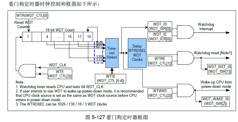
看门狗定时器的用途是在软件出问题时执行系统复位功能,这可以防止系统无限期地挂起。除此之外,看门狗定时器还支持将CPU 从掉电模式唤醒的功能。看门狗定时器包含一个18 位的自由运行计数器,定时溢出间隔可编程。
特征
18-位自由运行WDT 计数器用于看门狗定时器超时间隔。
可选择的超时间隔 (2^4 ~ 2^18),超时间隔为104 ms ~ 26.316 s (如果WDT_CLK = 10 kHz)。
复位周期 = (1 / 10 kHz) * 63,如果WDT_CLK = 10 kHz

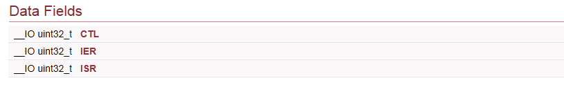
对应的寄存器是这个
#define WDT_BASE              (APB1PERIPH_BASE + 0x04000)    ///< WDT register base address

#define APB1PERIPH_BASE       ((uint32_t)0x40000000)    ///< APB1 base address

#define CLK_APBCLK_WDT_EN_Pos (0) /*!< CLK_T::APBCLK: WDT_EN Position */
#define CLK_APBCLK_WDT_EN_Msk (0x1ul << CLK_APBCLK_WDT_EN_Pos) /*!< CLK_T::APBCLK: WDT_EN Mask
typedef struct {

/**
* PWRCTL
* ===================================================================================================
* Offset: 0x00 System Power Down Control Register
* ---------------------------------------------------------------------------------------------------
* |Bits |Field |Descriptions
* | :----: | :----: | :---- |
* |[0] |HXT_EN |HXT Control
* | | |This is a protected register. Please refer to open lock sequence to program it.
* | | |The bit default value is set by flash controller user configuration register config0 [26].
* | | |0 = Disabled.
* | | |1 = Enabled.
* | | |HXT is disabled by default.
* |[1] |LXT_EN |LXT Control
* | | |This is a protected register. Please refer to open lock sequence to program it.
* | | |0 = Disabled.
* | | |1 = Enabled.
* | | |LXT is disabled by default.
* |[2] |HIRC_EN |HIRC Control
* | | |This is a protected register. Please refer to open lock sequence to program it.
* | | |0 = Disabled.
* | | |1 = Enabled.
* | | |HIRC is enabled by default.
* |[3] |LIRC_EN |LIRC Control
* | | |This is a protected register. Please refer to open lock sequence to program it.
* | | |0 = Disabled.
* | | |1 = Enabled.
* | | |LIRC is enabled by default.
* |[4] |WK_DLY |Wake-Up Delay Counter Enable
* | | |This is a protected register. Please refer to open lock sequence to program it.
* | | |When chip wakes up from Power-down mode, the clock control will delay 4096 clock cycles to wait HXT stable or 16 clock cycles to wait HIRC stable.
* | | |0 = Delay clock cycle Disabled.
* | | |1 = Delay clock cycle Enabled.
* |[5] |PD_WK_IE |Power-Down Mode Wake-Up Interrupt Enable
* | | |This is a protected register. Please refer to open lock sequence to program it.
* | | |0 = Disabled.
* | | |1 = Enabled.
* | | |PD_WK_INT will be set if both PD_WK_IS and PD_WK_IE are high.
* |[6] |PD_EN |Chip Power-Down Mode Enable Bit
* | | |This is a protected register. Please refer to open lock sequence to program it.
* | | |When CPU sets this bit, the chip power down is enabled and chip will not enter Power-down mode until CPU sleep mode is also active
* | | |When chip wakes up from Power-down mode, this bit will be auto cleared.
* | | |When chip is in Power-down mode, the LDO, HXT and HIRC will be disabled, but LXT and LIRC are not controlled by Power-down mode.
* | | |When power down, the PLL and system clock (CPU, HCLKx and PCLKx) are also disabled no matter the Clock Source selection.
* | | |Peripheral clocks are not controlled by this bit, if peripheral Clock Source is from LXT or LIRC.
* | | |In Power-down mode, flash macro power is ON.
* | | |0 = Chip operated in Normal mode.
* | | |1 = Chip power down Enabled.
* |[8] |HXT_SELXT |HXT SELXT
* | | |This is a protected register. Please refer to open lock sequence to program it.
* | | |0 = High frequency crystal loop back path Disabled. It is used for external oscillator.
* | | |1 = High frequency crystal loop back path Enabled. It is used for external crystal.
* |[9] |HXT_GAIN |HXT Gain Control Bit
* | | |This is a protected register. Please refer to open lock sequence to program it.
* | | |Gain control is used to enlarge the gain of crystal to make sure crystal wok normally.
* | | |If gain control is enabled, crystal will consume more power than gain control off.
* | | |0 = Gain control Disabled. It means HXT gain is always high.
* | | |For 16MHz to 24MHz crystal.
* | | |1 = Gain control Enabled. HXT gain will be high lasting 2ms then low. This is for power saving.
* | | |For 4MHz to 16MHz crystal.
* |[10] |LXT_SCNT |LXT Stable Time Control
* | | |This is a protected register. Please refer to open lock sequence to program it.
* | | |0 = Delay 4096 LXT before LXT output.
* | | |1 = Delay 8192 LXT before LXT output.
* |[12:11] |HXT_HF_ST |HXT Frequency Selection
* | | |Set this bit to meet HXT frequency selection (Recommended)
* | | |00 = HXT frequency is from 4 MHz to 12 MHz.
* | | |01 = HXT frequency is from 12 MHz to 16 MHz.
* | | |10 = HXT frequency is from 16 MHz to 24 MHz.
* | | |11 = Reserved.
*/
__IO uint32_t PWRCTL;

/**
* AHBCLK
* ===================================================================================================
* Offset: 0x04 AHB Devices Clock Enable Control Register
* ---------------------------------------------------------------------------------------------------
* |Bits |Field |Descriptions
* | :----: | :----: | :---- |
* |[0] |GPIO_EN |GPIO Controller Clock Enable
* | | |0 = Disabled.
* | | |1 = Enabled.
* |[1] |DMA_EN |DMA Controller Clock Enable
* | | |0 = Disabled.
* | | |1 = Enabled.
* |[2] |ISP_EN |Flash ISP Controller Clock Enable
* | | |0 = Disabled.
* | | |1 = Enabled.
* |[3] |EBI_EN |EBI Controller Clock Enable
* | | |0 = Disabled.
* | | |1 = Enabled.
* |[4] |SRAM_EN |SRAM Controller Clock Enable
* | | |0 = Disabled.
* | | |1 = Enabled.
* |[5] |TICK_EN |System Tick Clock Enable
* | | |0 = Disabled.
* | | |1 = Enabled.
*/
__IO uint32_t AHBCLK;

/**
* APBCLK
* ===================================================================================================
* Offset: 0x08 APB Devices Clock Enable Control Register
* ---------------------------------------------------------------------------------------------------
* |Bits |Field |Descriptions
* | :----: | :----: | :---- |
* |[0] |WDT_EN |Watchdog Timer Clock Enable Control
* | | |This is a protected register. Please refer to open lock sequence to program it.
* | | |This bit is used to control the WDT APB clock only, The WDT engine Clock Source is from LIRC.
* | | |0 = Disabled.
* | | |1 = Enabled.
* |[1] |RTC_EN |Real-Time-Clock Clock Enable Control
* | | |This bit is used to control the RTC APB clock only, The RTC engine Clock Source is from LXT.
* | | |0 = Disabled.
* | | |1 = Enabled.
* |[2] |TMR0_EN |Timer0 Clock Enable Control
* | | |0 = Disabled.
* | | |1 = Enabled.
* |[3] |TMR1_EN |Timer1 Clock Enable Control
* | | |0 = Disabled.
* | | |1 = Enabled.
* |[4] |TMR2_EN |Timer2 Clock Enable Control
* | | |0 = Disabled.
* | | |1 = Enabled.
* |[5] |TMR3_EN |Timer3 Clock Enable Control
* | | |0 = Disabled.
* | | |1 = Enabled.
* |[6] |FDIV_EN |Frequency Divider Output Clock Enable Control
* | | |0 = Disabled.
* | | |1 = Enabled.
* |[7] |SC2_EN |SmartCard 2 Clock Enable Control
* | | |0 = Disabled.
* | | |1 = Enabled.
* |[8] |I2C0_EN |I2C0 Clock Enable Control
* | | |0 = Disabled.
* | | |1 = Enabled.
* |[9] |I2C1_EN |I2C1 Clock Enable Control
* | | |0 = Disabled.
* | | |1 = Enabled.
* |[12] |SPI0_EN |SPI0 Clock Enable Control
* | | |0 = Disabled.
* | | |1 = Enabled.
* |[13] |SPI1_EN |SPI1 Clock Enable Control
* | | |0 = Disabled.
* | | |1 = Enabled.
* |[14] |SPI2_EN |SPI2 Clock Enable Control
* | | |0 = Disabled.
* | | |1 = Enabled.
* |[16] |UART0_EN |UART0 Clock Enable Control
* | | |0 = Disabled.
* | | |1 = Enabled.
* |[17] |UART1_EN |UART1 Clock Enable Control
* | | |0 = Disabled.
* | | |1 = Enabled.
* |[20] |PWM0_CH01_EN|PWM0 Channel 0 And Channel 1Clock Enable Control
* | | |0 = Disabled.
* | | |1 = Enabled.
* |[21] |PWM0_CH23_EN|PWM0 Channel 2 And Channel 3 Clock Enable Control
* | | |0 = Disabled.
* | | |1 = Enabled.
* |[22] |PWM1_CH01_EN|PWM1 Channel 0 And Channel 1 Clock Enable Control
* | | |0 = Disabled.
* | | |1 = Enabled.
* |[23] |PWM1_CH23_EN|PWM1 Channel 2 And Channel 3 Clock Enable Control
* | | |0 = Disabled.
* | | |1 = Enabled.
* |[25] |DAC_EN |12-Bit DAC Clock Enable Control
* | | |0 = Disabled.
* | | |1 = Enabled.
* |[26] |LCD_EN |LCD Controller Clock Enable Control
* | | |0 = Disabled.
* | | |1 = Enabled.
* |[27] |USBD_EN |USB FS Device Controller Clock Enable Control
* | | |0 = Disabled.
* | | |1 = Enabled.
* |[28] |ADC_EN |Analog-Digital-Converter (ADC) Clock Enable Control
* | | |0 = Disabled.
* | | |1 = Enabled.
* |[29] |I2S_EN |I2S Clock Enable Control
* | | |0 = Disabled.
* | | |1 = Enabled.
* |[30] |SC0_EN |SmartCard 0 Clock Enable Control
* | | |0 = Disabled.
* | | |1 = Enabled.
* |[31] |SC1_EN |SmartCard 1 Clock Enable Control
* | | |0 = Disabled.
* | | |1 = Enabled.
*/
__IO uint32_t APBCLK;

/**
* CLKSTATUS
* ===================================================================================================
* Offset: 0x0C Clock status monitor Register
* ---------------------------------------------------------------------------------------------------
* |Bits |Field |Descriptions
* | :----: | :----: | :---- |
* |[0] |HXT_STB |HXT Clock Source Stable Flag
* | | |0 = HXT clock is not stable or not enable.
* | | |1 = HXT clock is stable.
* |[1] |LXT_STB |LXT Clock Source Stable Flag
* | | |0 = LXT clock is not stable or not enable.
* | | |1 = LXT clock is stable.
* |[2] |PLL_STB |PLL Clock Source Stable Flag
* | | |0 = PLL clock is not stable or not enable.
* | | |1 = PLL clock is stable.
* |[3] |LIRC_STB |LIRC Clock Source Stable Flag
* | | |0 = LIRC clock is not stable or not enable.
* | | |1 = LIRC clock is stable.
* |[4] |HIRC_STB |HIRC Clock Source Stable Flag
* | | |0 = HIRC clock is not stable or not enable.
* | | |1 = HIRC clock is stable.
* |[7] |CLK_SW_FAIL|Clock Switch Fail Flag
* | | |0 = Clock switch success.
* | | |1 = Clock switch fail.
* | | |This bit will be set when target switch Clock Source is not stable. This bit is write 1 clear
*/
__I uint32_t CLKSTATUS;

/**
* CLKSEL0
* ===================================================================================================
* Offset: 0x10 Clock Source Select Control Register 0
* ---------------------------------------------------------------------------------------------------
* |Bits |Field |Descriptions
* | :----: | :----: | :---- |
* |[2:0] |HCLK_S |HCLK Clock Source Selection
* | | |This is a protected register. Please refer to open lock sequence to program it.
* | | |Note:
* | | |Before Clock Source switches, the related clock sources (pre-select and new-select) must be turn on
* | | |The 3-bit default value is reloaded with the value of CFOSC (Config0[26:24]) in user configuration register in Flash controller by any reset.
* | | |Therefore the default value is either 000b or 111b.
* | | |000 = HXT
* | | |001 = LXT
* | | |010 = PLL Clock
* | | |011 = LIRC
* | | |111 = HIRC
* | | |Others = Reserved
*/
__IO uint32_t CLKSEL0;

/**
* CLKSEL1
* ===================================================================================================
* Offset: 0x14 Clock Source Select Control Register 1
* ---------------------------------------------------------------------------------------------------
* |Bits |Field |Descriptions
* | :----: | :----: | :---- |
* |[1:0] |UART_S |UART 0/1 Clock Source Selection (UART0 And UART1 Use The Same Clock Source Selection)
* | | |00 = HXT
* | | |01 = LXT
* | | |10 = PLL Clock
* | | |11 = HIRC
* |[3:2] |ADC_S |ADC Clock Source Selection
* | | |00 = HXT
* | | |01 = LXT
* | | |10 = PLL Clock
* | | |11 = HIRC
* |[5:4] |PWM0_CH01_S|PWM0 Channel 0 And Channel 1 Clock Source Selection
* | | |PWM0 channel 0 and channel 1 use the same Engine clock source, both of them with the same prescaler
* | | |00 = HXT
* | | |01 = LXT
* | | |10 = HCLK
* | | |11 = HIRC
* |[7:6] |PWM0_CH23_S|PWM0 Channel 2 And Channel 3 Clock Source Selection
* | | |PWM0 channel 2 and channel 3 use the same Engine clock source, both of them with the same prescaler
* | | |00 = HXT
* | | |01 = LXT
* | | |10 = HCLK
* | | |11 = HIRC
* |[10:8] |TMR0_S |Timer0 Clock Source Selection
* | | |000 = HXT
* | | |001 = LXT
* | | |010 = LIRC
* | | |011 = External Pin
* | | |111 = HIRC
* | | |Others = Reserved
* |[14:12] |TMR1_S |Timer1 Clock Source Selection
* | | |000 = HXT
* | | |001 = LXT
* | | |010 = LIRC
* | | |011 = External Pin
* | | |111 = HIRC
* | | |Others = Reserved
* |[18] |LCD_S |LCD Clock Source Selection
* | | |0 = Clock Source from LXT.
* | | |1 = Reserved.
*/
__IO uint32_t CLKSEL1;

/**
* CLKSEL2
* ===================================================================================================
* Offset: 0x18 Clock Source Select Control Register 2
* ---------------------------------------------------------------------------------------------------
* |Bits |Field |Descriptions
* | :----: | :----: | :---- |
* |[3:2] |FRQDIV_S |Clock Divider Clock Source Selection
* | | |00 = HXT
* | | |01 = LXT
* | | |10 = HCLK
* | | |11 = HIRC
* |[5:4] |PWM1_CH01_S|PWM1 Channel 0 And Channel 1 Clock Source Selection
* | | |PWM1 channel 0 and channel 1 use the same Engine clock source, both of them with the same pre-scale
* | | |00 = HXT
* | | |01 = LXT
* | | |10 = HCLK
* | | |11 = HIRC
* |[7:6] |PWM1_CH23_S|PWM1 Channel 2 And Channel 2 Clock Source Selection
* | | |PWM1 channel 2 and channel 3 use the same Engine clock source, both of them with the same pre-scale
* | | |00 = HXT
* | | |01 = LXT
* | | |10 = HCLK
* | | |11 = HIRC
* |[10:8] |TMR2_S |Timer2 Clock Source Selection
* | | |000 = HXT
* | | |001 = LXT
* | | |010 = LIRC
* | | |011 = External Pin
* | | |111 = HIRC
* | | |Others = Reserved
* |[14:12] |TMR3_S |Timer3 Clock Source Selection
* | | |000 = HXT
* | | |001 = LXT
* | | |010 = LIRC
* | | |011 = External Pin
* | | |111 = HIRC
* | | |Others = Reserved
* |[17:16] |I2S_S |I2S Clock Source Selection
* | | |00 = HXT
* | | |01 = PLL Clock
* | | |10 = HIRC
* | | |11 = HIRC
* |[19:18] |SC_S |SC Clock Source Selection
* | | |00 = HXT
* | | |01 = PLL Clock
* | | |10 = HIRC
* | | |11 = HIRC
* | | |Note: SC0,SC1 and SC2 use the same Clock Source selection but they have different clock divider number.
* |[20] |SPI0_S |SPI0 Clock Source Selection
* | | |0 = PLL.
* | | |1 = HCLK.
* |[21] |SPI1_S |SPI1 Clock Source Selection
* | | |0 = PLL.
* | | |1 = HCLK.
* |[22] |SPI2_S |SPI2 Clock Source Selection
* | | |0 = PLL.
* | | |1 = HCLK.
*/
__IO uint32_t CLKSEL2;

/**
* CLKDIV0
* ===================================================================================================
* Offset: 0x1C Clock Divider Number Register 0
* ---------------------------------------------------------------------------------------------------
* |Bits |Field |Descriptions
* | :----: | :----: | :---- |
* |[3:0] |HCLK_N |HCLK Clock Divide Number From HCLK Clock Source
* | | |The HCLK clock frequency = (HCLK Clock Source frequency) / (HCLK_N + 1).
* |[7:4] |USB_N |USB Clock Divide Number From PLL Clock
* | | |The USB clock frequency = (PLL frequency ) / (USB_N + 1).
* |[11:8] |UART_N |UART Clock Divide Number From UART Clock Source
* | | |The UART clock frequency = (UART Clock Source frequency ) / (UART_N + 1).
* |[15:12] |I2S_N |I2S Clock Divide Number From I2S Clock Source
* | | |The I2S clock frequency = (I2S Clock Source frequency ) / (I2S_N + 1).
* |[23:16] |ADC_N |ADC Clock Divide Number From ADC Clock Source
* | | |The ADC clock frequency = (ADC Clock Source frequency ) / (ADC_N + 1).
* |[31:28] |SC0_N |SC 0 Clock Divide Number From SC 0 Clock Source
* | | |The SC 0 clock frequency = (SC0 Clock Source frequency ) / (SC0_N + 1).
*/
__IO uint32_t CLKDIV0;

/**
* CLKDIV1
* ===================================================================================================
* Offset: 0x20 Clock Divider Number Register 1
* ---------------------------------------------------------------------------------------------------
* |Bits |Field |Descriptions
* | :----: | :----: | :---- |
* |[3:0] |SC1_N |SC 1 Clock Divide Number From SC 1 Clock Source
* | | |The SC 1 clock frequency = (SC 1 Clock Source frequency ) / (SC1_N + 1).
* |[7:4] |SC2_N |SC 2 Clock Divide Number From SC2 Clock Source
* | | |The SC 2 clock frequency = (SC 2 Clock Source frequency ) / (SC2_N + 1).
*/
__IO uint32_t CLKDIV1;

/**
* PLLCTL
* ===================================================================================================
* Offset: 0x24 PLL Control Register
* ---------------------------------------------------------------------------------------------------
* |Bits |Field |Descriptions
* | :----: | :----: | :---- |
* |[4:0] |FB_DV |PLL Feedback Divider Control Pins
* | | |Refer to the formulas below the table.
* | | |The range of FB_DV is from 0 to 63.
* |[9:8] |IN_DV |PLL Input Divider Control Pins
* | | |Refer to the formulas below the table.
* |[12] |OUT_DV |PLL Output Divider Control Pins
* | | |Refer to the formulas below the table. This bit MUST be 0 for PLL output low deviation.
* |[16] |PD |Power-Down Mode
* | | |If set the PD_EN bit "1" in PWR_CTL register, the PLL will enter Power-down mode too
* | | |0 = PLL is in normal mode.
* | | |1 = PLL is in power-down mode (default).
* |[17] |PLL_SRC |PLL Source Clock Select
* | | |0 = PLL source clock from HXT.
* | | |1 = PLL source clock from HIRC.
*/
__IO uint32_t PLLCTL;

/**
* FRQDIV
* ===================================================================================================
* Offset: 0x28 Frequency Divider Control Register
* ---------------------------------------------------------------------------------------------------
* |Bits |Field |Descriptions
* | :----: | :----: | :---- |
* |[3:0] |FSEL |Divider Output Frequency Selection Bits
* | | |The formula of output frequency is
* | | |Fout = Fin/2^(N+1),.
* | | |Where Fin is the input clock frequency, Fout is the frequency of divider output clock and N is the 4-bit value of FSEL[3:0].
* |[4] |FDIV_EN |Frequency Divider Enable Bit
* | | |0 = Frequency Divider Disabled.
* | | |1 = Frequency Divider Enabled.
*/
__IO uint32_t FRQDIV;

/**
* MCLKO
* ===================================================================================================
* Offset: 0x2C Module Clock Output Register
* ---------------------------------------------------------------------------------------------------
* |Bits |Field |Descriptions
* | :----: | :----: | :---- |
* |[5:0] |MCLK_SEL |Module Clock Output Source Selection (PC.0)
* | | |000000 = ISP_CLK
* | | |000001 = HIRC
* | | |000010 = HXT
* | | |000011 = LXT
* | | |000100 = LIRC
* | | |000101 = PLL output
* | | |000110 = PLL input
* | | |000111 = System Tick
* | | |001000 = HCLK clock
* | | |001010 = PCLK clock
* | | |100000 = TMR0_CLK
* | | |100001 = TMR1_CLK
* | | |100010 = UART0_CLK
* | | |100011 = USB_CLK
* | | |100100 = ADC_CLK
* | | |100101 = WDT_CLK
* | | |100110 = PWM0_CH01_CLK
* | | |100111 = PWM0_CH32_CLK
* | | |101001 = LCD_CLK
* | | |111000 = TMR2_CLK
* | | |111001 = TMR3_CLK
* | | |111010 = UART1_CLK
* | | |111011 = PWM1_CH01_CLK
* | | |111100 = PWM1_CH23_CLK
* | | |111101 = I²S_CLK
* | | |111110 = SC0_CLK
* | | |111111 = SC1_CLK
* |[7] |MCLK_EN |Module Clock Output Enable
* | | |User can get the module clock output from PC.0 pin via choosing the clock source in the MCLK_SEL bit field and then setting MCLK_EN bit to 1.
* | | |0 = Module clock output Disabled.
* | | |1 = Module clock output Enabled.
* | | |Note: If this bit is enabled, PC.0 will be configured to module clock output and the setting of PC0_MFP will be ineffective
*/
__IO uint32_t MCLKO;

/**
* WK_INTSTS
* ===================================================================================================
* Offset: 0x30 Wake-up interrupt status
* ---------------------------------------------------------------------------------------------------
* |Bits |Field |Descriptions
* | :----: | :----: | :---- |
* |[0] |PD_WK_IS |Wake-Up Interrupt Status In Chip Power-Down Mode
* | | |This bit indicates that some event resumes chip from Power-down mode
* | | |The status is set if external interrupts, UART, GPIO, RTC, USB, SPI, Timer, WDT, and BOD wake-up occurred.
* | | |Write 1 to clear this bit.
*/
__IO uint32_t WK_INTSTS;

} CLK_T;
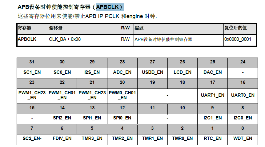
对照datasheet,只需要看APBCLK的部分就可以了。
功能描述
看门狗定时器的用途是在软件出问题时执行系统复位功能,这可以防止系统无限期地挂起。除此之外,看门狗定时器还支持将CPU 从掉电模式唤醒的功能,
此外当 CPU 进入掉电模式时,WDT 计数器会自动重置。
看门狗定时器包含一个18 位的自由运行计数器,定时溢出间隔可编程。
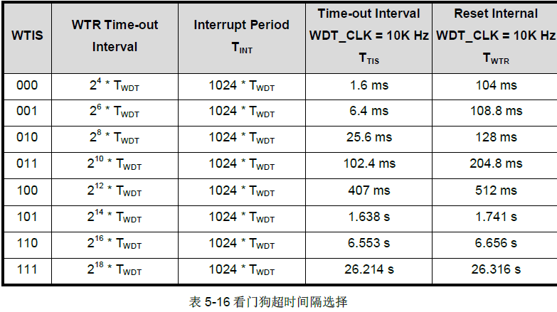
接下来的表格给出了看门狗超时间隔选择,
而接下来的图片给出了看门狗中断信号和复位信号的时序。
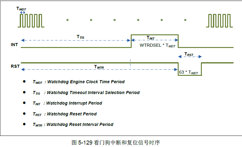
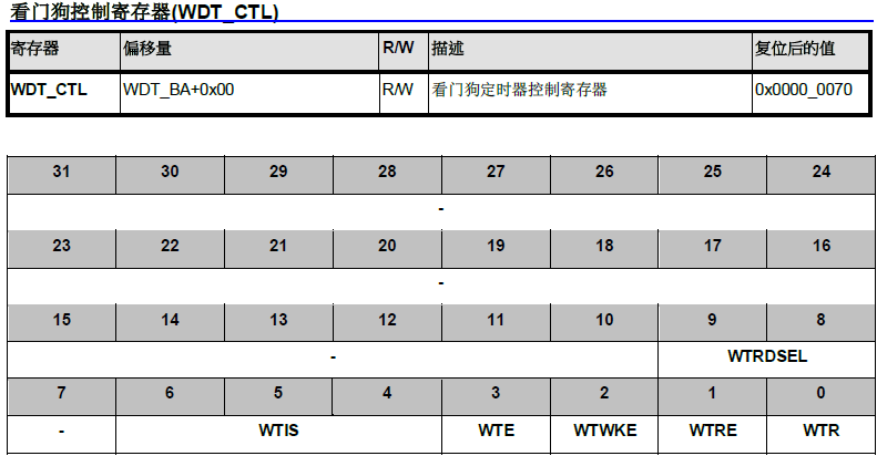
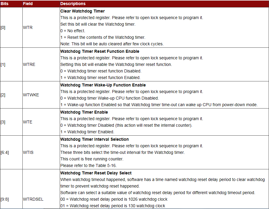
设置 WTE (WDT_CTL[3]) 使能看门狗定时器和WDT 计数器开始计数。
当计数器达到选择的超时间隔,看门狗定时器中断标志WDT_IS 将被立即被置位,并请求WDT 中断 (如果看门狗定时器中断使能位WDT_IE 置位),同时紧接着超时事件会有一个指定的延时可透过 WTRDSEL 設置,用户必须在该指定延时过期前设置WTR (WDT_CTL[0]) (看门狗定时器复位) 为高来复位18 位 WDT 计数器,以防止芯片复位。
WTR 位在WDT 计数器复位后由硬件自动清零。
通过设置WTIS (WDT_CTL[6:4]),有8 种带指定延时时间的超时间隔可供选择(上面的表格)。
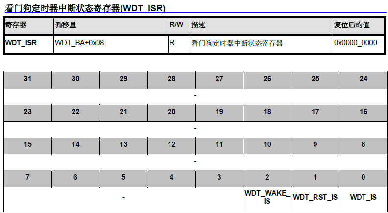
如果在指定延迟时间过期后,WDT 计数器没有被清零,看门狗定时器将置位看门狗定时器复位标志(WDT_RST_IS),并复位CPU。
这个复位将持续63 个 WDT 时钟 (TRST),然后芯片重启,并从复位向量(0x0000_0000) 处重新开始执行程序。
WDT_RST_IS 不会被看门狗复位清零。用户可用软件轮询WDT_RST_IS 来识别复位源是否WDT。
明白了原理,再看一下它们的寄存器,然后找到对应的寄存器,就可以进行配置了
寄存器是什么?在我的理解就是地址,这个地址对应着硬件的
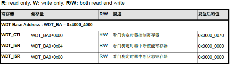
下图是寄存器的基地址和偏移地址:
对应的宏定义为:
#define APB1PERIPH_BASE       ((uint32_t)0x40000000)    ///< APB1 base address

#define WDT_BASE              (APB1PERIPH_BASE + 0x04000)    ///< WDT register base address
#define WDT                   ((WDT_T *) WDT_BASE)              ///< Pointer to WDT register structure
上文是WDT的基地址,也就是WDT_BA的部分,而下面是它的寄存器对应地址

typedef struct {
/**
* CTL
* ===================================================================================================
* Offset: 0x00 Watchdog Timer Control Register
* ---------------------------------------------------------------------------------------------------
* |Bits |Field |Descriptions
* | :----: | :----: | :---- |
* |[0] |WTR |Clear Watchdog Timer
* | | |This is a protected register. Please refer to open lock sequence to program it.
* | | |Set this bit will clear the Watchdog timer.
* | | |0 = No effect.
* | | |1 = Reset the contents of the Watchdog timer.
* | | |Note: This bit will be auto cleared after few clock cycles.
* |[1] |WTRE |Watchdog Timer Reset Function Enable
* | | |This is a protected register. Please refer to open lock sequence to program it.
* | | |Setting this bit will enable the Watchdog timer reset function.
* | | |0 = Watchdog timer reset function Disabled.
* | | |1 = Watchdog timer reset function Enabled.
* |[2] |WTWKE |Watchdog Timer Wake-Up Function Enable
* | | |This is a protected register. Please refer to open lock sequence to program it.
* | | |0 = Watchdog timer Wake-up CPU function Disabled.
* | | |1 = Wake-up function Enabled so that Watchdog timer time-out can wake up CPU from power-down mode.
* |[3] |WTE |Watchdog Timer Enable
* | | |This is a protected register. Please refer to open lock sequence to program it.
* | | |0 = Watchdog timer Disabled (this action will reset the internal counter).
* | | |1 = Watchdog timer Enabled.
* |[6:4] |WTIS |Watchdog Timer Interval Selection
* | | |This is a protected register. Please refer to open lock sequence to program it.
* | | |These three bits select the time-out interval for the Watchdog timer.
* | | |This count is free running counter.
* | | |Please refer to the Table 5-16.
* |[9:8] |WTRDSEL |Watchdog Timer Reset Delay Select
* | | |When watchdog timeout happened, software has a time named watchdog reset delay period to clear watchdog timer to prevent watchdog reset happened.
* | | |Software can select a suitable value of watchdog reset delay period for different watchdog timeout period.
* | | |00 = Watchdog reset delay period is 1026 watchdog clock
* | | |01 = Watchdog reset delay period is 130 watchdog clock
* | | |10 = Watchdog reset delay period is 18 watchdog clock
* | | |11 = Watchdog reset delay period is 3 watchdog clock
* | | |This register will be reset if watchdog reset happened
*/
__IO uint32_t CTL;
/**
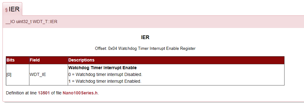
* IER
* ===================================================================================================
* Offset: 0x04 Watchdog Timer Interrupt Enable Register
* ---------------------------------------------------------------------------------------------------
* |Bits |Field |Descriptions
* | :----: | :----: | :---- |
* |[0] |WDT_IE |Watchdog Timer Interrupt Enable
* | | |0 = Watchdog timer interrupt Disabled.
* | | |1 = Watchdog timer interrupt Enabled.
*/
__IO uint32_t IER;
/**
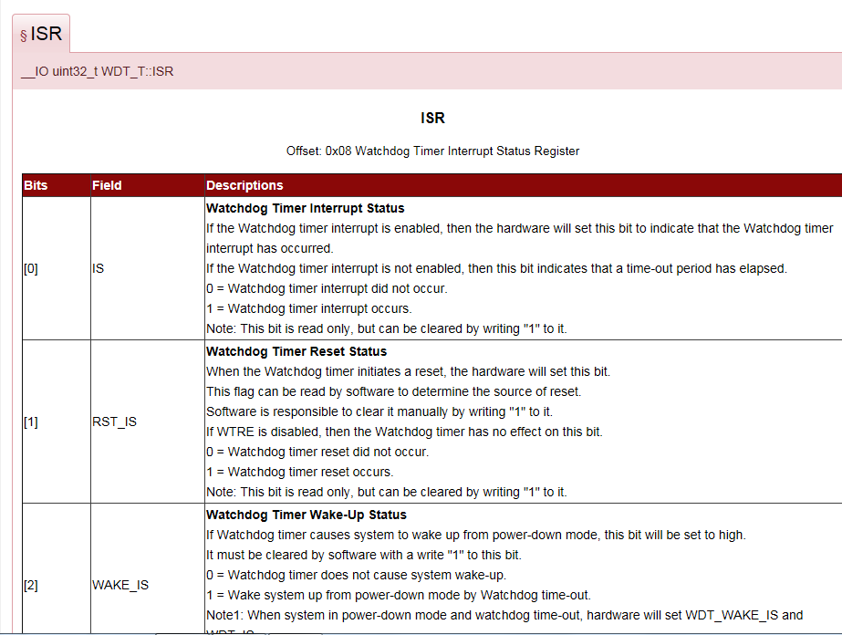
* ISR
* ===================================================================================================
* Offset: 0x08 Watchdog Timer Interrupt Status Register
* ---------------------------------------------------------------------------------------------------
* |Bits |Field |Descriptions
* | :----: | :----: | :---- |
* |[0] |IS |Watchdog Timer Interrupt Status
* | | |If the Watchdog timer interrupt is enabled, then the hardware will set this bit to indicate that the Watchdog timer interrupt has occurred.
* | | |If the Watchdog timer interrupt is not enabled, then this bit indicates that a time-out period has elapsed.
* | | |0 = Watchdog timer interrupt did not occur.
* | | |1 = Watchdog timer interrupt occurs.
* | | |Note: This bit is read only, but can be cleared by writing "1" to it.
* |[1] |RST_IS |Watchdog Timer Reset Status
* | | |When the Watchdog timer initiates a reset, the hardware will set this bit.
* | | |This flag can be read by software to determine the source of reset.
* | | |Software is responsible to clear it manually by writing "1" to it.
* | | |If WTRE is disabled, then the Watchdog timer has no effect on this bit.
* | | |0 = Watchdog timer reset did not occur.
* | | |1 = Watchdog timer reset occurs.
* | | |Note: This bit is read only, but can be cleared by writing "1" to it.
* |[2] |WAKE_IS |Watchdog Timer Wake-Up Status
* | | |If Watchdog timer causes system to wake up from power-down mode, this bit will be set to high.
* | | |It must be cleared by software with a write "1" to this bit.
* | | |0 = Watchdog timer does not cause system wake-up.
* | | |1 = Wake system up from power-down mode by Watchdog time-out.
* | | |Note1: When system in power-down mode and watchdog time-out, hardware will set WDT_WAKE_IS and WDT_IS.
* | | |Note2: After one engine clock, this bit can be cleared by writing "1" to it
*/
__IO uint32_t ISR;
} WDT_T;
#define WDT_CTL_WTR_Msk                  (0x1ul << WDT_CTL_WTR_Pos)                        /*!< WDT_T::CTL: WTR Mask                      */

#define WDT_CTL_WTRE_Pos                 (1)                                               /*!< WDT_T::CTL: WTRE Position                 */
#define WDT_CTL_WTRE_Msk                 (0x1ul << WDT_CTL_WTRE_Pos)                       /*!< WDT_T::CTL: WTRE Mask                     */

#define WDT_CTL_WTWKE_Pos                (2)                                               /*!< WDT_T::CTL: WTWKE Position                */
#define WDT_CTL_WTWKE_Msk                (0x1ul << WDT_CTL_WTWKE_Pos)                      /*!< WDT_T::CTL: WTWKE Mask                    */

#define WDT_CTL_WTE_Pos                  (3)                                               /*!< WDT_T::CTL: WTE Position                  */
#define WDT_CTL_WTE_Msk                  (0x1ul << WDT_CTL_WTE_Pos)                        /*!< WDT_T::CTL: WTE Mask                      */

#define WDT_CTL_WTIS_Pos                 (4)                                               /*!< WDT_T::CTL: WTIS Position                 */
#define WDT_CTL_WTIS_Msk                 (0x7ul << WDT_CTL_WTIS_Pos)                       /*!< WDT_T::CTL: WTIS Mask                     */

#define WDT_CTL_WTRDSEL_Pos              (8)                                               /*!< WDT_T::CTL: WTRDSEL Position              */
#define WDT_CTL_WTRDSEL_Msk              (0x3ul << WDT_CTL_WTRDSEL_Pos)                    /*!< WDT_T::CTL: WTRDSEL Mask                  */
//以上部分是否感到眼熟?跟WDT_CTL的地址是一一对应的,后面也是一样,也就是说0bit是WTR,1是WTRE.WTIS是第四位,但是它本身占三位,
//所以下一个寄存器就会移三位,又保留了一位,所以左移第八位。后面都是一样的
#define WDT_IER_IE_Pos (0) /*!< WDT_T::IER: IE Position */
#define WDT_IER_IE_Msk (0x1ul << WDT_IER_IE_Pos) /*!< WDT_T::IER: IE Mask */

#define WDT_ISR_IS_Pos (0) /*!< WDT_T::ISR: IS Position */
 #define WDT_ISR_IS_Msk (0x1ul << WDT_ISR_IS_Pos) /*!< WDT_T::ISR: IS Mask */

#define WDT_ISR_RST_IS_Pos (1) /*!< WDT_T::ISR: RST_IS Position */

#define WDT_ISR_RST_IS_Msk (0x1ul << WDT_ISR_RST_IS_Pos) /*!< WDT_T::ISR: RST_IS Mask */

#define WDT_ISR_WAKE_IS_Pos (2) /*!< WDT_T::ISR: WAKE_IS Position */ #
define WDT_ISR_WAKE_IS_Msk (0x1ul << WDT_ISR_WAKE_IS_Pos) /*!< WDT_T::ISR: WAKE_IS Mask */

/**@}*/
 /* WDT_CONST */

/**@}*/

/* end of WDT register group */

上面是它的最底层部分,您看懂了么?其实就是强制地址转换,分配地址,然后根据地址进行。配置寄存器就是给他们一个输入,或者输出。不过虽然本质就是这样,但操作并不简单,
因为他们的寄存器很多,而且大多要涉及外围电路和外部器件,任何一个环节出错,都不可能达到效果,虽然麻烦,但大部分都是有规律的。
这里穿插一则寄存器的小知识

在存储器 Block2 这块区域,设计的是片上外设,它们以四个字节为一个单元,共32bit,每一个单元对应不同的功能,当我们控制这些单元时就可以驱动外设工作。
我们可以找到每个单元的起始地址,然后通过 C语言指针的操作方式来访问这些单元,如果每次都是通过这种地址的方式来访问,不仅不好记忆还容易出错,
这时我们可以根据每个单元功能的不同,以功能为名给这个内存单元取一个别名,这个别名就是我们经常说的寄存器,
这个给已经分配好地址的有特定功能的内存单元取别名的过程就叫寄存器映射。

当然寄存器有软件的也有硬件的,电路方面在我的新浪博客上面会有描述。
再插一则小知识,是关于强制类型转换的
关于一个
int *ptr=(int *)(&a+1)
问题的探讨
网络上看到这样一道有意思的题目,是关于数组与指针的问题,描述如下:
main()
{
int a[5]={1,2,3,4,5};
int *ptr=(int *)(&a+1);
printf("%d,%d",*(a+1),*(ptr-1));
}
输出为:2,5
请解释以上代码的输出结果。答案如下:
*(a+1)其实很简单就是指a[1],输出为2. 问题关键就在于第二个点,
*(ptr-1)输出为多少?
解释如下,&a+1不是首地址+1,系统会认为加了一个整个a数组,偏移了整个数组a的大小(也就是5个int的大小)。所以
int *ptr=(int *)(&a+1);其实ptr实际是&(a[5]),也就是a+5. 原因为何呢?
&a是数组指针,其类型为int(*)[5]; 而指针加1要根据指针类型加上一定的值,不同类型的指针+1之后增加的大小不同,
a是长度为5的int数组指针,所以要加5*sizeof(int),所以ptr实际是a[5],但是ptr与(&a+1)类型是不一样的,这点非常重要,所以ptr-1只会减去sizeof(int*),
a,&a的地址是一样的,但意思就不一样了,a是数组首地址,也就是a[0]的地址,&a是对象(数组)首地址,a+1是数组下一元素的地址,即a[1],&a+1是下一个对象的地址,即a[5]。
小端:低地址存放低位数据;
大端:低地址存放高位数据;
而网络中传输是用大端。
用代码实现大小端利用了共用体的原理实现判断是比较简单的一个方法:
由于共用体中的所有元素都存放在一块内存空间中,而b的起始地址是从int型的起始地址对齐的。所以对一个int型的数据进行写1,如果是大端的话,char型的b就会为1,否则b就为0.
接下来,我们再来看看,上面所包含的寄存器,这是一个很大的量,请耐心看完,相信会有收获的。
既然我们熟悉了底层。那么我们当然不会止步于此,应用层的东西,当然也要做。
在功能描述那一章节时,我们其实已经明白了,它的具体操作和步骤,但是为了我们更加清楚明白和方便调用,我们决定采用库函数的形式,来讲述这个应用,首先我想说的是这只是一个小的官方例程,如果后续会有大型的项目,不涉及保密的话,我会把它共享出来
既然我们要用看门狗,既然要使用它,我们当然要打开它,即进行初始化。
首先选择时钟
void SYS_Init(void)
{

    /*---------------------------------------------------------------------------------------------------------*/
    /* Init System Clock                                                                                       */
    /*---------------------------------------------------------------------------------------------------------*/
    /* Unlock protected registers */
    SYS_UnlockReg();

    /* Enable External XTAL (4~24 MHz) */
    CLK_EnableXtalRC(CLK_PWRCTL_HXT_EN_Msk);

    /* Enable LIRC */
    CLK_EnableXtalRC(CLK_PWRCTL_LIRC_EN_Msk);

    /* Waiting for 12MHz clock ready */
    CLK_WaitClockReady( CLK_CLKSTATUS_HXT_STB_Msk);

    /* Waiting for LIRC clock ready */
    CLK_WaitClockReady( CLK_CLKSTATUS_LIRC_STB_Msk);

    /* Switch HCLK clock source to HXT */
    CLK_SetHCLK(CLK_CLKSEL0_HCLK_S_HXT,CLK_HCLK_CLK_DIVIDER(1));

    /* Enable IP clock */
    CLK_EnableModuleClock(UART0_MODULE);
    CLK_EnableModuleClock(WDT_MODULE);
/*
#define WDT_MODULE ((1UL<<31)|(3<<29)|(MODULE_NoMsk<<25)|( 0<<20)|(0<<18)|(MODULE_NoMsk<<10)|( 0<<5)|CLK_APBCLK_WDT_EN_Pos )
/*!< Watchdog Timer Module */
#define MODULE_NoMsk 0x0 /*!< Not mask on MODULE index */
#define WDT_MODULE ((1UL<<31)|(3<<29)|(MODULE_NoMsk<<25)|( 0<<20)|(0<<18)|(MODULE_NoMsk<<10)|( 0<<5)|CLK_APBCLK_WDT_EN_Pos )
#define CLK_APBCLK_WDT_EN_Pos (0) /*!< CLK_T::APBCLK: WDT_EN Position */
#define CLK_APBCLK_WDT_EN_Msk (0x1ul << CLK_APBCLK_WDT_EN_Pos) /*!< CLK_T::APBCLK: WDT_EN Mask
*/
/* Select IP clock source */
    CLK_SetModuleClock(UART0_MODULE, CLK_CLKSEL1_UART_S_HXT, CLK_UART_CLK_DIVIDER(1));
    CLK_SetModuleClock(WDT_MODULE, 0, 0);

    /* Update System Core Clock */
    /* User can use SystemCoreClockUpdate() to calculate SystemCoreClock. */
    SystemCoreClockUpdate();


    /*---------------------------------------------------------------------------------------------------------*/
    /* Init I/O Multi-function                                                                                 */
    /*---------------------------------------------------------------------------------------------------------*/
    /* Set GPB multi-function pins for UART0 RXD and TXD */
    SYS->PB_L_MFP &= ~(SYS_PB_L_MFP_PB0_MFP_Msk | SYS_PB_L_MFP_PB1_MFP_Msk);
    SYS->PB_L_MFP |= (SYS_PB_L_MFP_PB1_MFP_UART0_TX | SYS_PB_L_MFP_PB0_MFP_UART0_RX);
    /* Lock protected registers */
    SYS_LockReg();

}
void CLK_SetModuleClock(uint32_t u32ModuleIdx, uint32_t u32ClkSrc, uint32_t u32ClkDiv)
{
uint32_t u32tmp=0,u32sel=0,u32div=0;
if(MODULE_CLKDIV_Msk(u32ModuleIdx)!=MODULE_NoMsk) {u32div =(uint32_t)&CLK->CLKDIV0+((MODULE_CLKDIV(u32ModuleIdx))*4);u32tmp = *(volatile uint32_t *)(u32div);u32tmp = ( u32tmp & ~(MODULE_CLKDIV_Msk(u32ModuleIdx)<<MODULE_CLKDIV_Pos(u32ModuleIdx)) ) | u32ClkDiv;*(volatile uint32_t *)(u32div) = u32tmp;}
#define MODULE_CLKDIV_Msk(x) ((x >>10) & 0xff) /*!< Calculate CLKDIV mask offset on MODULE index */
#define MODULE_CLKDIV_Msk(x) ((x >>10) & 0xff) /*!< Calculate CLKDIV mask offset on MODULE index */
#define MODULE_CLKDIV_Pos(x) ((x >>5 ) & 0x1f) /*!< Calculate CLKDIV position offset on MODULE index */
#define MODULE_CLKDIV_Pos(x) ((x >>5 ) & 0x1f) /*!< Calculate CLKDIV position offset on MODULE index */
( u32tmp & ~(MODULE_CLKDIV_Msk(u32ModuleIdx)<<MODULE_CLKDIV_Pos(u32ModuleIdx)) ) | u32ClkDiv;
~((1110 0000 0000 0000 0000 0000 0000>>10) <<(1110 0000 0000 0000 0000 0000 >>5))|u32Div mingbaile zhongyv
// 1110 0000 0000 0000 0000 0000 0000 0000 右移5位为0000 1110 0000 0000 0000 0000 0000 0000 0000
// 1110 0000 0000 0000 0000 0000 0000 0000 右移10位为 0000 0000 0111 0000 0000 0000 0000 0000 0000
//所谓模块就是给时钟的WDT_EN位一个使能
if(MODULE_CLKSEL_Msk(u32ModuleIdx)!=MODULE_NoMsk) {u32sel = (uint32_t)&CLK->CLKSEL0+((MODULE_CLKSEL(u32ModuleIdx))*4);u32tmp = *(volatile uint32_t *)(u32sel);u32tmp = ( u32tmp & ~(MODULE_CLKSEL_Msk(u32ModuleIdx)<<MODULE_CLKSEL_Pos(u32ModuleIdx)) ) | u32ClkSrc;*(volatile uint32_t *)(u32sel) = u32tmp;}}
即我们刚开始所讲的设置 WTE (WDT_CTL[3]) 使能看门狗定时器和WDT 计数器开始计数。(在功能描述那一部分第一句)
/*** @brief This function make WDT module start counting with different time-out interval* @param[in] u32TimeoutInterval Time-out interval period of WDT module. Valid values are:* - \ref WDT_TIMEOUT_2POW4* - \ref WDT_TIMEOUT_2POW6* - \ref WDT_TIMEOUT_2POW8* - \ref WDT_TIMEOUT_2POW10* - \ref WDT_TIMEOUT_2POW12* - \ref WDT_TIMEOUT_2POW14* - \ref WDT_TIMEOUT_2POW16* - \ref WDT_TIMEOUT_2POW18* @param[in] u32ResetDelay Reset delay period while WDT time-out happened. Valid values are:* - \ref WDT_RESET_DELAY_3CLK* - \ref WDT_RESET_DELAY_18CLK* - \ref WDT_RESET_DELAY_130CLK* - \ref WDT_RESET_DELAY_1026CLK* @param[in] u32EnableReset Enable WDT reset system function. Valid values are TRUE and FALSE* @param[in] u32EnableWakeup Enable WDT wake-up system function. Valid values are TRUE and FALSE* @return None*/
void  WDT_Open(uint32_t u32TimeoutInterval,
               uint32_t u32ResetDelay,
               uint32_t u32EnableReset,
               uint32_t u32EnableWakeup)
{

    WDT->CTL = u32TimeoutInterval | u32ResetDelay | WDT_CTL_WTE_Msk |
               (u32EnableReset << WDT_CTL_WTRE_Pos) |
               (u32EnableWakeup << WDT_CTL_WTWKE_Pos);
    return;
}
这个意思就是选择它的超时时间,和复位延迟时间和启动系统功能,和复位系统功能
u32TimeoutInterval WDT模块的超时间隔时间。有效值是:
* - \ ref WDT_TIMEOUT_2POW4
* - \ ref WDT_TIMEOUT_2POW6
* - \ ref WDT_TIMEOUT_2POW8
* - \ ref WDT_TIMEOUT_2POW10
* - \ ref WDT_TIMEOUT_2POW12
* - \ ref WDT_TIMEOUT_2POW14
* - \ ref WDT_TIMEOUT_2POW16
* - \ ref WDT_TIMEOUT_2POW18
* @param [in] u32ResetDelay发生WDT超时的复位延迟时间。有效值是:
* - \ ref WDT_RESET_DELAY_3CLK
* - \ ref WDT_RESET_DELAY_18CLK
* - \ ref WDT_RESET_DELAY_130CLK
* - \ ref WDT_RESET_DELAY_1026CLK
* @param [in] u32EnableReset启用WDT复位系统功能。有效值为TRUE和FALSE
* @param [in] u32EnableWakeup启用WDT唤醒系统功能。有效值为TRUE和FALSE
* @返回无
* /
对应的库函数与表格分别是:
#define WDT_TIMEOUT_2POW4           (0UL << WDT_CTL_WTIS_Pos) /*!< WDT setting for timeout interval = 2^4 * WDT clocks */
#define WDT_TIMEOUT_2POW6           (1UL << WDT_CTL_WTIS_Pos) /*!< WDT setting for timeout interval = 2^6 * WDT clocks */
#define WDT_TIMEOUT_2POW8           (2UL << WDT_CTL_WTIS_Pos) /*!< WDT setting for timeout interval = 2^8 * WDT clocks */
#define WDT_TIMEOUT_2POW10          (3UL << WDT_CTL_WTIS_Pos) /*!< WDT setting for timeout interval = 2^10 * WDT clocks */
#define WDT_TIMEOUT_2POW12          (4UL << WDT_CTL_WTIS_Pos) /*!< WDT setting for timeout interval = 2^12 * WDT clocks */
#define WDT_TIMEOUT_2POW14          (5UL << WDT_CTL_WTIS_Pos) /*!< WDT setting for timeout interval = 2^14 * WDT clocks */
#define WDT_TIMEOUT_2POW16          (6UL << WDT_CTL_WTIS_Pos) /*!< WDT setting for timeout interval = 2^16 * WDT clocks */
#define WDT_TIMEOUT_2POW18          (7UL << WDT_CTL_WTIS_Pos) /*!< WDT setting for timeout interval = 2^18 * WDT clocks */

#define WDT_RESET_DELAY_3CLK        (3UL << WDT_CTL_WTRDSEL_Pos)    /*!< WDT setting reset delay to 3 WDT clocks */
#define WDT_RESET_DELAY_18CLK       (2UL << WDT_CTL_WTRDSEL_Pos)    /*!< WDT setting reset delay to 18 WDT clocks */
#define WDT_RESET_DELAY_130CLK      (1UL << WDT_CTL_WTRDSEL_Pos)    /*!< WDT setting reset delay to 130 WDT clocks */
#define WDT_RESET_DELAY_1026CLK     (0UL << WDT_CTL_WTRDSEL_Pos)    /*!< WDT setting reset delay to 1026 WDT clocks */
我们看一看第二句:
当计数器达到选择的超时间隔,看门狗定时器中断标志WDT_IS将被立即被置位,并请求WDT 中断 (如果看门狗定时器中断使能位WDT_IE 置位),同时紧接着超时事件会有一个指定的延时可透过 WTRDSEL 設置,用户必须在该指定延时过期前设置WTR (WDT_CTL[0]) (看门狗定时器复位) 为高来复位18 位 WDT 计数器,以防止芯片复位。
请求中断就得先有中断,使能中断:
/**
* @brief This function enables the WDT time-out interrupt
* @param None
* @return None
*/
__STATIC_INLINE void WDT_EnableInt(void)
{
    WDT->IER = WDT_IER_IE_Msk;
    return;
}
/**
\brief Enable External Interrupt
\details Enables a device-specific interrupt in the NVIC interrupt controller.
\param [in] IRQn External interrupt number. Value cannot be negative.
*/
__STATIC_INLINE void NVIC_EnableIRQ(IRQn_Type IRQn)
{
NVIC->ISER[0U] = (uint32_t)(1UL << (((uint32_t)(int32_t)IRQn) & 0x1FUL));
}
这两个中断,一个是WDT使能中断,一个是外部中断。我们还要利用定时器进行喂狗操作,所谓喂狗:
void WDT_IRQHandler(void)
{
// Clear WDT interrupt flag
WDT_CLEAR_TIMEOUT_INT_FLAG();
// Check WDT wake up flag
if(WDT_GET_TIMEOUT_WAKEUP_FLAG()) {
printf("Wake up by WDT\n");
// Clear WDT wake up flag
WDT_CLEAR_TIMEOUT_WAKEUP_FLAG();
}
}
这里面涉及的库函数有下面这些:看完您是否明白了?
#define WDT_ISR_WAKE_IS_Msk (0x1ul << WDT_ISR_WAKE_IS_Pos) /*!< WDT_T::ISR: WAKE_IS Mask */
#define WDT_GET_TIMEOUT_WAKEUP_FLAG() (WDT->ISR & WDT_ISR_WAKE_IS_Msk ? 1 : 0)
#define WDT_CLEAR_TIMEOUT_WAKEUP_FLAG() (WDT->ISR = WDT_ISR_WAKE_IS_Msk)
那么?功能与描述最后这一句,WDT_RST_IS 不会被看门狗复位清零。用户可用软件轮询WDT_RST_IS 来识别复位源是否WDT。
然后,上今天的主菜,主程序上场:
/******************************************************************************
 * @file     main.c
 * @version  V1.00
 * $Revision: 3 $
 * $Date: 14/09/11 7:39p $
 * @brief    Use WDT to wake up system from Power-down mode periodically.
 *
 * @note
 * Copyright (C) 2013-2014 Nuvoton Technology Corp. All rights reserved.
 *****************************************************************************/
#include <stdio.h>
#include "Nano100Series.h"


void WDT_IRQHandler(void)
{


    // Clear WDT interrupt flag
    WDT_CLEAR_TIMEOUT_INT_FLAG();

    // Check WDT wake up flag
    if(WDT_GET_TIMEOUT_WAKEUP_FLAG()) {
        printf("Wake up by WDT\n");
        // Clear WDT wake up flag
        WDT_CLEAR_TIMEOUT_WAKEUP_FLAG();
    }

}


void SYS_Init(void)
{

    /*---------------------------------------------------------------------------------------------------------*/
    /* Init System Clock                                                                                       */
    /*---------------------------------------------------------------------------------------------------------*/
    /* Unlock protected registers */
    SYS_UnlockReg();

    /* Enable External XTAL (4~24 MHz) */
    CLK_EnableXtalRC(CLK_PWRCTL_HXT_EN_Msk);

    /* Enable LIRC */
    CLK_EnableXtalRC(CLK_PWRCTL_LIRC_EN_Msk);

    /* Waiting for 12MHz clock ready */
    CLK_WaitClockReady( CLK_CLKSTATUS_HXT_STB_Msk);

    /* Waiting for LIRC clock ready */
    CLK_WaitClockReady( CLK_CLKSTATUS_LIRC_STB_Msk);

    /* Switch HCLK clock source to HXT */
    CLK_SetHCLK(CLK_CLKSEL0_HCLK_S_HXT,CLK_HCLK_CLK_DIVIDER(1));

    /* Enable IP clock */
    CLK_EnableModuleClock(UART0_MODULE);
    CLK_EnableModuleClock(WDT_MODULE);


    /* Select IP clock source */
    CLK_SetModuleClock(UART0_MODULE, CLK_CLKSEL1_UART_S_HXT, CLK_UART_CLK_DIVIDER(1));
    CLK_SetModuleClock(WDT_MODULE, 0, 0);

    /* Update System Core Clock */
    /* User can use SystemCoreClockUpdate() to calculate SystemCoreClock. */
    SystemCoreClockUpdate();


    /*---------------------------------------------------------------------------------------------------------*/
    /* Init I/O Multi-function                                                                                 */
    /*---------------------------------------------------------------------------------------------------------*/
    /* Set GPB multi-function pins for UART0 RXD and TXD */
    SYS->PB_L_MFP &= ~(SYS_PB_L_MFP_PB0_MFP_Msk | SYS_PB_L_MFP_PB1_MFP_Msk);
    SYS->PB_L_MFP |= (SYS_PB_L_MFP_PB1_MFP_UART0_TX | SYS_PB_L_MFP_PB0_MFP_UART0_RX);
    /* Lock protected registers */
    SYS_LockReg();

}


int32_t main (void)
{
    /* Init System, IP clock and multi-function I/O
       In the end of SYS_Init() will issue SYS_LockReg()
       to lock protected register. If user want to write
       protected register, please issue SYS_UnlockReg()
       to unlock protected register if necessary */
    SYS_Init();

    /* Init UART to 115200-8n1 for print message */
    UART_Open(UART0, 115200);

    printf("\nThis sample code demonstrate using WDT to wake system up from power down mode\n");

    // WDT register is locked, so it is necessary to unlock protect register before configure WDT
    SYS_UnlockReg();

    // WDT timeout every 2^14 WDT clock, disable system reset, enable wake up system
    WDT_Open(WDT_TIMEOUT_2POW14, 0, FALSE, TRUE);

    // Enable WDT timeout interrupt
    WDT_EnableInt();
    NVIC_EnableIRQ(WDT_IRQn);

    while(1) {
        // Wait 'til UART FIFO empty to get a cleaner console out
        while(!UART_IS_TX_EMPTY(UART0));
        CLK_PowerDown();
    }

}

/*** (C) COPYRIGHT 2014 Nuvoton Technology Corp. ***/
这其中还有一些我没有讲的太清楚,放心,我会让各位都清楚明白的,我会慢慢去修正,欢迎您的指点
失败正常,跌倒也正常,但是丧失了自信和斗志,只会沉沦,永远见不到太阳。常常幻想有一天我怎样怎样,但是梦醒来的时候,却发现自己一无所有,要想得到,还得继续奔跑。